Or better: input(1).raw.sized(1.um).merged(2).output("corner")
@Matthias: The documentation mentions the example layer.sized(300.nm).raw.merged(2), but am I right to say that this example is wrong? In the example of the "corner" above, it seems necessary to put the raw operator before the sized operator, not after.
But none of the proposed method (euclidian, square, projection, whole-edges) can catch the fact that either the width, either the space is not enough at the common corner.
Putting "raw" after "sized" works, if the polygons are not touching. In this case, the sizing would be applied individually and using raw post-size makes the sized polygons not being merged. Hence "merged(2)" gives the overlap. Putting "raw" before "sized" will not make the polygons merged before size even if they touch, so you would detect butting-polygon cases too (polygons that share edges, not just points).
The reason why "raw" after "sized" is not working here is a different one: the kissing corner situation is recognized as "coherent" and the two rectangles are merged into a single polygon. Hence "sized" would not create overlapping parts there.
There is a switch inside KLayout's "Region" object to control this ("min coherence"), but unfortunately it's not recognized by "sized". You can force a pre-size merge and then go to raw mode:
And to answer the second question: yes, it's normal that "layer.merged" gives one polygon for kissing corner cases, because "min_coherence" is false by default.
@laurent_c: thanks for the suggestion. Width doesn't give a marker here as the edges involved don't face towards each other with their inner sides. I'm afraid a solution is possible only by special treatment of this case inside "width".
For your information: I have provided a fix in the master and will release a 0.25.9 soon which has this fix ported. After this, the kissing corners will be reported as width or space violations.
That sounds good! However, I would add this comment: "touching corners" are legal patterns, they can be accepted by mask shops. They should not necessarily be thought as illegal.
Ocasta, you are right for mask shops. But the foundries will refuse to process with such shapes on your circuit, because it does not pass their DRC.
Laurent
the foundries will refuse to process with such shapes on your circuit
No, this depends on the DRM of the foundry. I wrote my previous remark after checking that such "kissing corner" pattern was indeed present on MPW wafers made by a certain foundry in Belgium.
I know that both happens: sometimes these pattern are legal, sometimes the aren't. In the sense of "connected" figures they are legal, because a connection cannot be guaranteed. But on implant layers they are perfectly legal, because there is no connection implied and they do not comprise a manufacturing issue like resist failures.
But I think that most tools will flag them as illegal, so there is a certain compatibility then.
I actually thought about making the feature configurable. But you can essentially disable it already by using "projection" metrics:
layer.width(100.nm, projection)   # does not report kissing corners
# will report kissing corners:
layer.width(100.nm)
layer.width(100.nm, square)
layer.width(100.nm, euclidian)

Comments
Apply a sizing and check for an overlap?
https://www.klayout.de/doc-qt4/about/drc_ref_layer.html
Like:
input(1).sized(1.um).width(3.um).output("corner")Or better:
input(1).raw.sized(1.um).merged(2).output("corner")@Matthias: The documentation mentions the example
layer.sized(300.nm).raw.merged(2), but am I right to say that this example is wrong? In the example of the "corner" above, it seems necessary to put therawoperator before thesizedoperator, not after.Thank you Ocasta. I was using the standard checks :
But none of the proposed method (euclidian, square, projection, whole-edges) can catch the fact that either the width, either the space is not enough at the common corner.
Laurent
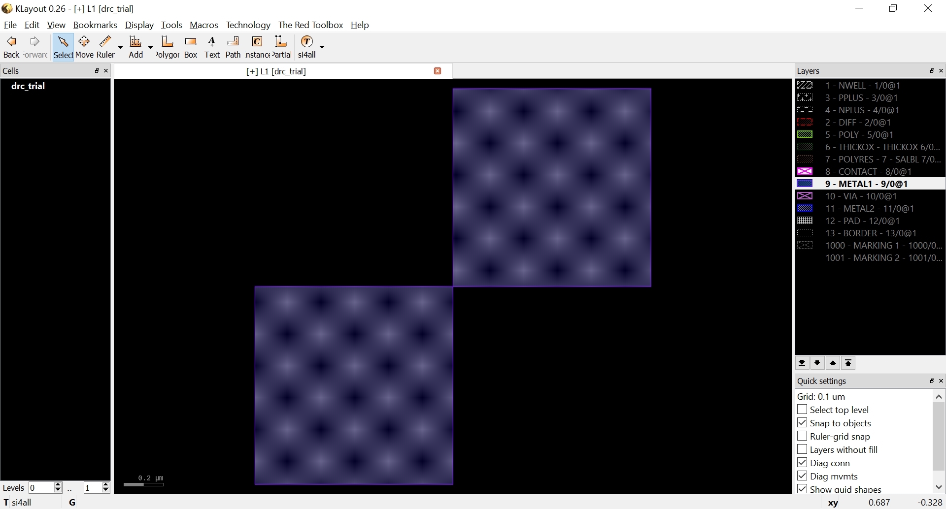
@Matthias: When two shapes are touching at only one corner point...
layer.mergedgives one unique single shape?layer.merged(2)gives nothing?Oh well ... the famous "kissing corner" problem.
@ocasta:
Putting "raw" after "sized" works, if the polygons are not touching. In this case, the sizing would be applied individually and using raw post-size makes the sized polygons not being merged. Hence "merged(2)" gives the overlap. Putting "raw" before "sized" will not make the polygons merged before size even if they touch, so you would detect butting-polygon cases too (polygons that share edges, not just points).
The reason why "raw" after "sized" is not working here is a different one: the kissing corner situation is recognized as "coherent" and the two rectangles are merged into a single polygon. Hence "sized" would not create overlapping parts there.
There is a switch inside KLayout's "Region" object to control this ("min coherence"), but unfortunately it's not recognized by "sized". You can force a pre-size merge and then go to raw mode:
And to answer the second question: yes, it's normal that "layer.merged" gives one polygon for kissing corner cases, because "min_coherence" is false by default.
@laurent_c: thanks for the suggestion. Width doesn't give a marker here as the edges involved don't face towards each other with their inner sides. I'm afraid a solution is possible only by special treatment of this case inside "width".
Kind regards,
Matthias
For information, here is the way I solved it :
Laurent
For your information: I have provided a fix in the master and will release a 0.25.9 soon which has this fix ported. After this, the kissing corners will be reported as width or space violations.
Regards,
Matthias
That sounds good! However, I would add this comment: "touching corners" are legal patterns, they can be accepted by mask shops. They should not necessarily be thought as illegal.
Ocasta, you are right for mask shops. But the foundries will refuse to process with such shapes on your circuit, because it does not pass their DRC.
Laurent
No, this depends on the DRM of the foundry. I wrote my previous remark after checking that such "kissing corner" pattern was indeed present on MPW wafers made by a certain foundry in Belgium.
I know that both happens: sometimes these pattern are legal, sometimes the aren't. In the sense of "connected" figures they are legal, because a connection cannot be guaranteed. But on implant layers they are perfectly legal, because there is no connection implied and they do not comprise a manufacturing issue like resist failures.
But I think that most tools will flag them as illegal, so there is a certain compatibility then.
I actually thought about making the feature configurable. But you can essentially disable it already by using "projection" metrics:
Which looks kind of consistent to me.
Regards,
Matthias