Howdy, Stranger!
It looks like you're new here. If you want to get involved, click one of these buttons!
Quick Links
Reduce split gate option in LVS

Hi all,
I check reduction split gate option in Klayout.
Case 1: I use nand2x2 cell
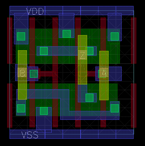
Extracted circuit:
M$1 5 2 1 8 PCH L=0.04U W=0.55U AS=0.0495P AD=0.0385P PS=1.185U PD=0.83U
M$3 5 3 1 8 PCH L=0.04U W=0.55U AS=0.04125P AD=0.05225P PS=0.85U PD=1.205U
M$5 4 2 6 9 NCH L=0.04U W=0.255U AS=0.02535P AD=0.01785P PS=0.73U PD=0.395U
M$6 6 2 7 9 NCH L=0.04U W=0.255U AS=0.01785P AD=0.01785P PS=0.395U PD=0.395U
M$7 7 3 1 9 NCH L=0.04U W=0.255U AS=0.01785P AD=0.0204P PS=0.395U PD=0.415U
M$8 1 3 4 9 NCH L=0.04U W=0.255U AS=0.0204P AD=0.02535P PS=0.415U PD=0.73U
After reduction:
M$1 5 2 1 7 PCH L=0.04U W=0.55U AS=0.0495P AD=0.0385P PS=1.185U PD=0.83U
M$3 5 3 1 7 PCH L=0.04U W=0.55U AS=0.04125P AD=0.05225P PS=0.85U PD=1.205U
M$5 4 2 6 8 NCH L=0.04U W=0.51U AS=0.0432P AD=0.0357P PS=1.125U PD=0.79U
M$7 4 3 1 8 NCH L=0.04U W=0.51U AS=0.03825P AD=0.04575P PS=0.81U PD=1.145U
this option works perfectly in this case !!!!
Case 2: I use nand2x4 cell
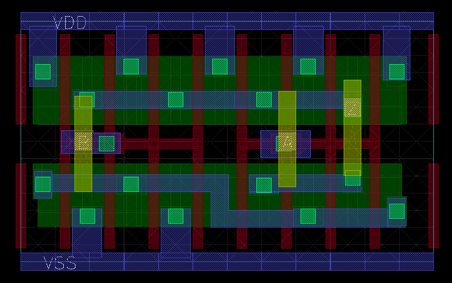
After reduction:
M$1 6 1 3 7 PCH L=0.04U W=1.1U AS=0.088P AD=0.077P PS=2.015U PD=1.66U
M$5 6 2 3 7 PCH L=0.04U W=1.1U AS=0.077P AD=0.088P PS=1.66U PD=2.015U
M$9 4 1 5 8 NCH L=0.04U W=0.765U AS=0.06155P AD=0.05355P PS=1.52U PD=1.185U
M$12 5 1 9 8 NCH L=0.04U W=0.255U AS=0.01785P AD=0.01785P PS=0.395U PD=0.395U
M$13 9 2 3 8 NCH L=0.04U W=0.255U AS=0.01785P AD=0.01785P PS=0.395U PD=0.395U
M$14 3 2 4 8 NCH L=0.04U W=0.765U AS=0.05355P AD=0.06105P PS=1.185U PD=1.52U
But target netlist:
M$1 6 1 4 7 PCH L=0.04U W=1.1U AS=0.088P AD=0.077P PS=2.015U PD=1.66U
M$5 6 2 4 7 PCH L=0.04U W=1.1U AS=0.077P AD=0.088P PS=1.66U PD=2.015U
M$9 3 1 5 8 NCH L=0.04U W=1.02U AS=0.0794P AD=0.0714P PS=1.915U PD=1.58U
M$13 3 2 4 8 NCH L=0.04U W=1.02U AS=0.0714P AD=0.0789P PS=1.58U PD=1.915U
This option does not work perfectly in this case. It is only reduced for PMOS (PCH) and NMOS is not thorough. Can you help me fix this problem ?
Thank you very much
Comments
Hi,
The second case is lacking the symmetry requirement: there are basically two separate nodes in the low-side branch on the nand (the two serial transistors). But they are not interchangeable as one node is between two 3x transistors while the other one is between two 1x transistors.
Formally this prevents the reduction algorithm to join these nodes. There is no easy fix except for extending the algorithm. But I have no good idea how to do this currently. An option is to create a virtual connection through labels (use 'connect_implicict("nand2x4", "your_label")').
Matthias
Thank you so much for your information
Hi,
to resolve the issue i read netlist and join_net to joint the points like that, after that use device combine again. it work like expected. Here is my script
dai