Import Gerber PCB Files
Gerber PCB import allows creating GDS layout data from Gerber PCB files or to add Gerber files to GDS files as new layers. The import function supports a majority of the RS274X features for artwork files and a couple of different formats for the drill files. The importer will take a set of files and convert them to layout geometry. The importer offers some functionality to adjust the data appropriately, i.e. to define output layers and apply geometrical transformations. Another basic capability is to merge the geometry of a layer to remove overlaps and join paths into larger polygons.
Because of the manifold options, the import specification can become pretty complex. Therefore, it can be saved into a file (suggested suffix is ".pcb") in XML format which contains the importer specifications. Once such a file is created, KLayout can read this file like usual stream files (i.e. it can be specified on the command line) and use it as a recipe to import the associated Gerber files.
The PCB import function is available in the "File" menu ("Import/Gerber PCB"). Different entry points are provided that start a new project, open an existing project or to continue with the last project.
The basic workflow to import PCB data is:
- Specify the directory where the PCB data files are located (the "base" directory).
- Specify the import mode (the destination of the layout data).
- Decide about the layer mapping mode: free layer mapping or metal stack mapping. Free layer mapping allows an arbitrary mapping between PCB layers and GDS layers. This specification is the most flexible one but is tedious to enter. Metal stack mapping is easier to specify but confined to mapping a set of PCB files to a metal/via/metal stack scheme.
- Specify the files, GDS layers and PCB to GDS layer mapping.
- Specify a transformation if desired, either by specifying mapping points or a transformation directly.
- Decide about further options (i.e. merging, database unit, top cell name etc.).
The basic decision is how to specify the layer mapping. In free mode, the specification requires these steps:
- Specify the files to load (in the dialog on the "Files" page).
- Specify a list of output layers.
- Fill the input to output mapping matrix which assigns one or many output layers to each input file.
In layer stack mode, the specification workflow consists of these steps:
- Specify the GDS layer stack (the complete stack available for mapping PCB data into). The idea is basically to put another set of series of metal/via/metal layers on top of the GDS layer stack. The PCB layer closest to the die surface is placed into the first metal layer which is supposed to be the first above the on-chip layers.
- When the GDS layers are set, specify how many metal and drill hole files the PCB file set contains and whether the chip will be mounted on the top or bottom of the PCB. The latter decides in which order the PCB layers are assigned to GDS layers (remember, the first GDS layer will be the PCB layer closest to the die surface).
- Enter file names for the artwork files corresponding to metal layers.
- Specify file names for the drill files and what metal layers are connected by the (plated) drill holes. Since a drill hole can connect multiple layers in the stack, a connection information is always of the type "from metal, to metal" with the drill holes connecting all metal layers between "from" and "to".
The import dialog
The import dialog is organized in multiple pages that reflect the workflow for the import specification. On every page, the "File" menu button allows saving the current settings as a PCB import project, to open an existing project or to create a new project and to restart from scratch.

The first page offers some basic options:
- Base directory: this is the directory where all the PCB files are found. Not necessarily all files must be located there but are looked for relative to this directory. If all files are moved, just the base directory must change. The base directory is not stored in a project file. Instead, the base directory is the directory where the project file is stored. Basically this implies, that all data files will be referred to relative to the project file.
- Import mode: PCB data can be imported into the current layout (into the current cell). Usually, it this case, layers will be added to the current layout. Alternatively, a layout can be created which will be either placed into a new panel or added to the current panel.
- Layer mapping mode: Specify here whether to use free or layer stack mode. Check the box to use free layer mapping mode.
The layer stack flow
In the layer stack flow, on the first page, a sequence of metal and via layers must be specified. The assignment of metal and via layers is done automatically. The sequence is always a metal layer followed by a via layer. The number of layers must be odd so the last layer is a metal layer again. Via layers will connect the adjacent metal layers only.
Use the "+" button to add new layers. Move layers by selecting them and moving them up or down with the arrow buttons. Use the "X" button to remove all selected layers.
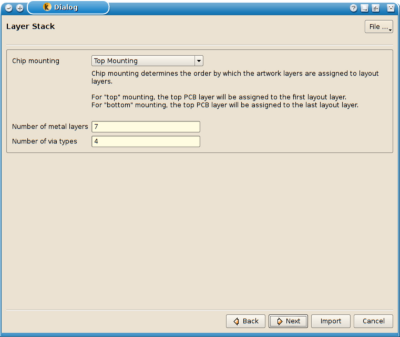
On the next page, the number of artwork and drill files needs to be specified. Later, the actual files need to be entered and assigned to metal or via layers. In addition the chip mounting position needs to be specified. In "top mounting" mode, it is assumed that the chip is placed surface down on the top (first) PCB layer. Thus the first metal above the chip stack will be the top PCB layer. In "bottom mounting" mode, the last PCB metal layer will be the first metal layer above the chip stack.
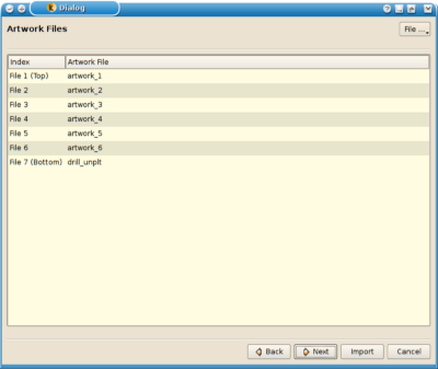
On the "Artwork Files" page, the artfile file names must be entered. They are automatically assigned to the respective metal layers. The assignment order depends on the mounting mode.
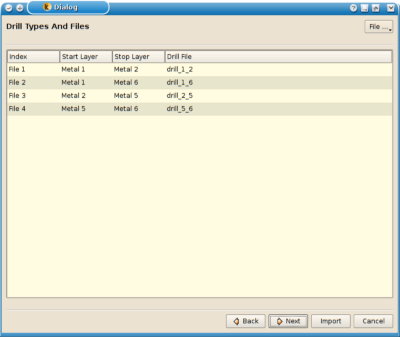
On the "Drill Files" page, the drill file names must be entered. Each drill file describes a certain drill step, which can connect multiple metal layers. On this page, this specification must be made. The first and last metal layer connected by the plated hole must be specified. The corresponding via layers will then be used to create via shapes.
The free layer mapping flow
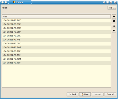
On the "Files" page, all PCB data files must be specified. This includes artwork and drill files. The order is not important but it is recommended to follow the physical stacking. This simplifies the assignment to GDS layers later. Use the arrow buttons to move the selected entries up or down. Use the "X" button to delete files from the list and use the "+" button to add new files.
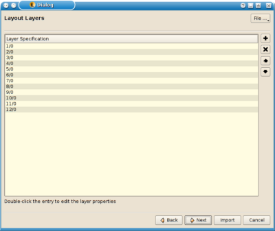
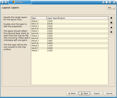
On the "Layout Layers" page all target layers must be specified. Provide a list with all layers that are used as target layers for the import. Again, the order is not important but maintaining a technological order will simplify the assignment in the next step. As on the previous page use the arrow buttons to move selected entries and the "+" and "X" button to add new entries and deleted the selected ones.
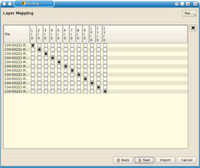
On the "Layer Mapping" page, each file can be assigned to one or may GDS layers. The assignment is described in form of a matrix where an "x" means that the file or layer given by the row is imported into the layer given by the column. A file can be imported into multiple layers which basically will duplicate the shapes. Click at the boxes to set or reset the mark. Use the "X" button on the left to reset all marks for the rows selected.
General options
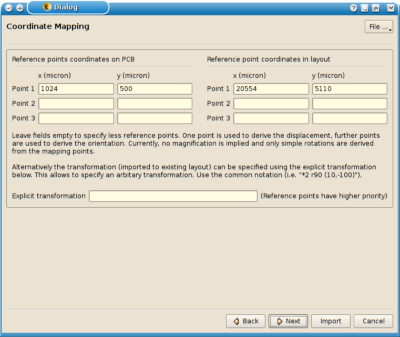
The "Coordinate Mapping" page allows specification of the transformation of the PCB data into the GDS space. Since PCB and GDS rarely share the origin, a transformation can be specified which is applied to the shapes when importing them.
A specification can be made in two ways:
- By specifying matching points: The transformation will be computed such that the given PCB coordinates are mapped to the given GDS coordinates. Up to three coordinate pairs can be given. If one coordinate pair is given, a displacement is derived. If two coordinate pairs are given, the rotation is computed as well (only multiples of 90 degree are supported currently). If three coordinate pairs are give, the algorithm can derive mirroring as well.
- By explicitly specifying the transformation: The transformation can be specified explicitly in
the lower entry field. The format is "x,y" for a simple translation (x, y are given in micron units),
"rx" or "mx" for a rotation by the angle "x"
or mirroring at the line with angle "x" and "*x" for a magnification of "x". All specifications can be combined, i.e.
"r90 170,-5100" specifies a rotation by 90 degree and displacement by 170 micron in horizontal and -5.1 mm in vertical
direction.
For a comprehensive description of that string, see Transformations in KLayout.
Hint: Both specifications can be combined, i.e. one coordinate pair can be given to define the displacement and the rotation can be specified explicitly.
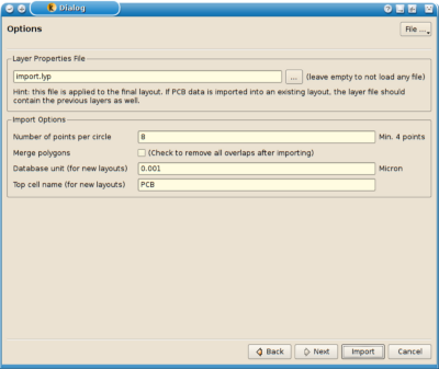
Finally, on the "Options" page, various options can be set:
- Layer properties file: If specified, this layer properties file will be loaded after the layers have been imported. The file is specified relative to the base directory.
- Number of points per circle: KLayout resolves the circular apertures commonly used in PCB layout into polygons to perform geometrical operations. This options allows choosing how many points will be used for the approximation of a full circle. Less points will mean less accurate representation but smaller polygons hence better performance on boolean operations used to compute clear areas for example.
- Merge polygons: If this option is set, all polygons will be joined if they overlap or touch. Note, that merging also happens implicitly if clear layers are used because the boolean operations used to cut out clear regions will implicitly merge the previous layout. This implicit merging cannot be disabled.
- Database unit and top cell name: This option allows choosing the database unit and top cell name for new layouts. This applies only, if the import mode implies a new layout.