Howdy, Stranger!
It looks like you're new here. If you want to get involved, click one of these buttons!
Quick Links
Metal perimeter to gate area ratio antenna rule

TSMC specifies their antenna rules as ratio between the area of the sidewalls of the metal lines to the area of the gate layer. As thickness of metal layer is constant per layer this effectively transforms the TSMC antenna rules to metal perimeter to gate area ratio limits.
Is this possible with the klayout DRC checker ?
Comments
I was already waiting for this request ...")
Technically that's not a big issue and code is prepared already for this. It's just not available yet as a DRC option. I have prepared a ticket for this: https://github.com/KLayout/klayout/issues/570
I'll try to include such an option in the next minor release.
BTW: how come you're porting TSMC rules to KLayout? I feel (from the feedback I get) that different users do the same here - maybe even on the same technology - but they can't share their work because the rules are confidential. That smells like duplicate work.
I'd support TSMC porting their rules in case they choose to approach me directly")
Regards,
Matthias
I just did a 0.18µm TSMC tape-out using Europractice as service. I don't have access to Calibre and had to do a few iterations to get antenna problems solved. At first sight I did not understand why there was a mismatch between antenna check results from klayout and the Calibre runs.
As open source EDA software developer I try to stay away from even the proprietary EDA software EULAs, especially so for Mentor Graphics.
Actually I am trying to solve the redoing of the work also with PDKMaster; anybody who wants to cooperate can contact me (email is in profile). I had a talk scheduled at FOSSistanbul; but this was cancelled last minute due to Corona.
As also indicated in a comment to the issue; I don't think current implementation can handle the TSMC antenna rules. The rules use only the perimeter of the metal to compute the ratio and does not use the area.
I have implemented "perimeter_only" now. It's going to go into the next minor release. The details are here: https://github.com/KLayout/klayout/issues/579
I hope TSMC appreciates that")
Matthias
Thanks, I guess TSMC will appreciate it as long they themselves don't have to support yet another EDA tool .
.
Hi Matthias
I have tried to write some antenna checks and indeed it seems to work.
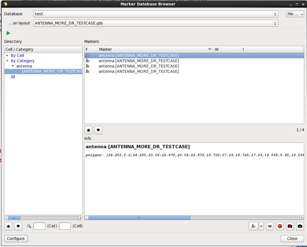
But one thing I am missing: is there a way to get actual area, perimeter, GATE area and diode areas of each violating net? I would like to put this info in the marker browser window, attached to each violation.
PS: I can attach a test case if needed.
Thanks!
Allon.
Hi Allon,
I'm sorry, but right now, the check will just output the metal layers. Plus, it will output the metal layers for all fails on the same layer, so you cannot differentiate the different nets. The tool is intended as a pass/fail check.
Matthias
OK. Thanks Matthias.