Howdy, Stranger!
It looks like you're new here. If you want to get involved, click one of these buttons!
Quick Links
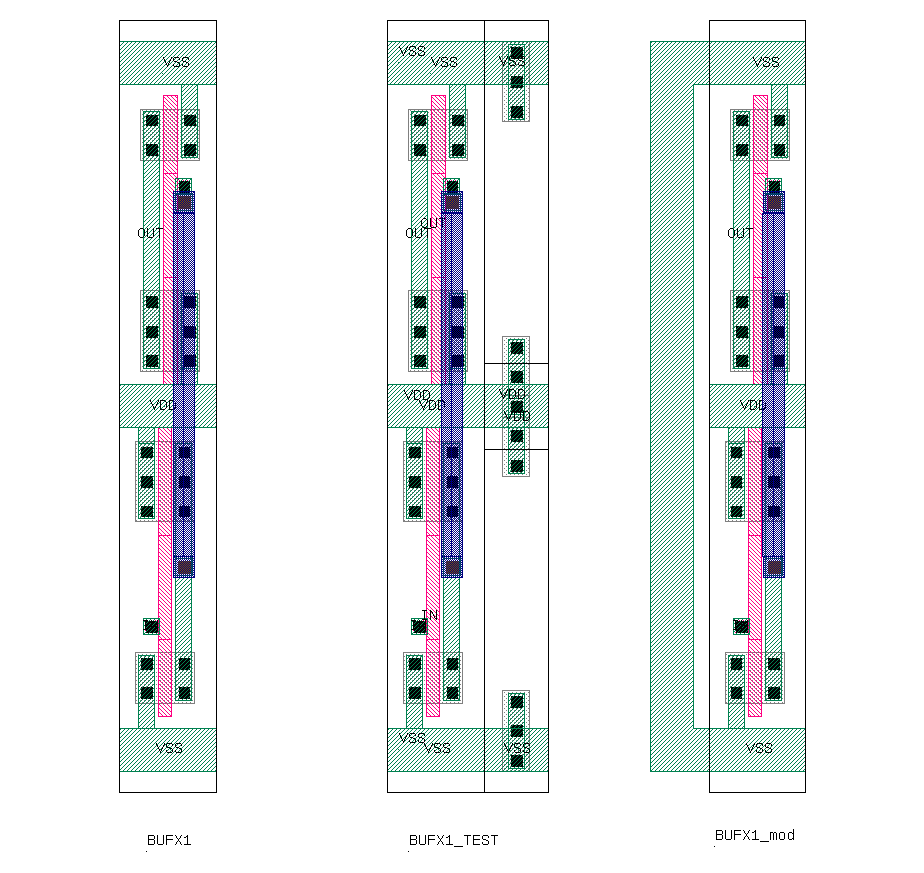
LVS for double height standard cell

Hi Matthias,
I tested LVS for double height standard cell by using sample data.
I made simple double height BUFX1 cell. --> (BUFX1)
Then I created test layout by adding 2 TIE cell. --> (BUFX1_TEST)
Source schematic "BUFX1_TEST"
.SUBCKT BUFX1_TEST OUT IN VDD VSS
X1 OUT IN VDD VSS VSS VDD BUFX1
.ENDS BUFX1_TEST
.SUBCKT BUFX1 OUT IN VDD VSS SUB NWELL
MP1 VDD IN NET1 NWELL PMOS L=0.25U W=1.5U
MP2 VDD NET1 OUT NWELL PMOS L=0.25U W=1.5U
MN1 VSS IN NET1 SUB NMOS L=0.25U W=0.95U
MN2 VSS NET1 OUT SUB NMOS L=0.25U W=0.95U
.ENDS BUFX1
Extracted net list
Though connect_implicit("VSS") was used, unknown "VSS$1" node was generated in BUFX1.
.SUBCKT BUFX1_TEST IN OUT VSS VDD
X$1 VDD VSS OUT VSS IN VSS VDD BUFX1
.ENDS BUFX1_TEST
.SUBCKT BUFX1 VDD VSS OUT VSS$1 IN SUB NWELL
M$1 VDD IN \$2 NWELL PMOS L=0.25U W=1.5U
M$2 VDD \$2 OUT NWELL PMOS L=0.25U W=1.5U
M$3 VSS IN \$2 SUB NMOS L=0.25U W=0.95U
M$4 VSS$1 \$2 OUT SUB NMOS L=0.25U W=0.95U
.ENDS BUFX1
Expected net list
This net list was only obtained by add metal1 data in BUFX1 cell to connect upper VSS and lower VSS. --> (BUFX1_mod)
.SUBCKT BUFX1_TEST IN OUT VSS VDD
X$1 VDD OUT VSS IN VSS VDD BUFX1
.ENDS BUFX1_TEST
.SUBCKT BUFX1 VDD OUT VSS IN SUB NWELL
M$1 VDD IN \$2 NWELL PMOS L=0.25U W=1.5U
M$2 VDD \$2 OUT NWELL PMOS L=0.25U W=1.5U
M$3 VSS IN \$2 SUB NMOS L=0.25U W=0.95U
M$4 VSS \$2 OUT SUB NMOS L=0.25U W=0.95U
.ENDS BUFX1
Can you confirm this result?
Thanks,
haru_f
Comments
Hi haru_f,
thank for you this nicely prepared material")
connect_implicit(...)acts on the top level only. This is a safety feature to avoid false matches due to virtual connections where physically they are missing.connect_implicit("VSS")worked as you can see: the BUFX1_TEST has one VSS net only.But "connect_implicit" does not act on the BUFX1 subcell, so it has two VSS pins. That's physically correct - you could basically connect the lower VSS to a different potential that the upper one. So having two pins is the correct representation.
I hope this explanation makes sense. As a general rule, the netlist KLayout produces will represent the physical topology of the cell and the same is expected from the corresponding schematic netlist's circuits.
Kind regards,
Matthias
Hi Matthias,
Thank you for the detailed explanation. Yes, I could make sense.
Actually, flat LVS verification was completed.
To run hierarchical LVS with double height standard cells,
is it possible to create new function and keyword "connect_inplicit_in_cell("node", "cellname"), for example ?
Example
connect_inplicit_in_cell("VSS", "BUFX1")
Thanks,
haru_f
I think this can be done - I have created a ticket for this: https://github.com/KLayout/klayout/issues/444
Although I need to say that this breaks with the concept of schematic/layout correspondence which is deeply built into the LVS implementation of KLayout.
Matthias
Hi Matthias,
Thank you for adding to the enhancement.
Thanks,
haru_f
Hi Matthias,
I could confirm this enhancement on my example data.
Thank you very much for your effort.
Best regards,
haru_f