Howdy, Stranger!
It looks like you're new here. If you want to get involved, click one of these buttons!
Quick Links
Reference Netlist Format

Hi Everybody,
I tried to make a reference netlist for xor2 gate like this but klayout doesn't understand.
Because xor2 gate use some dti_gen_inv and dti_gen_tx in some where with different Length of gate and Width of gate so I make it like sub netlist and use input parameter.
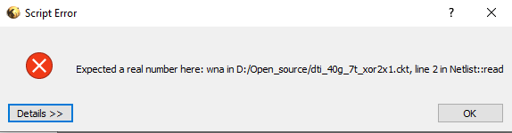
It show error:
How do i make it correct format?
.subckt dti_gen_tx VDD VSS PG NG IN OUT wna=0.3u wpa=0.3u
m1i2 IN NG OUT VSS nch l=0.04u w=wna
m1i3 IN PG OUT VDD pch l=0.04u w=wpa
.ends
.subckt dti_gen_inv VDD VSS A Z ln=0.04u lp=0.04u wn=0.3u wp=0.3u
m1i3 Z A VDD VDD pch l=lp w=wp
m1i4 Z A VSS VSS nch l=ln w=wn
.ends
.subckt dti_40g_7t_xor2x1 VDD VSS A Z B
x1i15 VDD VSS B N1N23 N1N56 N1N27 dti_gen_tx wna=0.255u wpa=0.275u
x1i55 VDD VSS A N1N56 dti_gen_inv ln=0.04u lp=0.04u wn=0.255u wp=0.275u
x1i57 VDD VSS N1N27 Z dti_gen_inv ln=0.04u lp=0.04u wn=0.255u wp=0.275u
x1i61 VDD VSS N1N23 B N1N58 N1N27 dti_gen_tx wna=0.255u wpa=0.275u
x1i62 VDD VSS N1N56 N1N58 dti_gen_inv ln=0.04u lp=0.04u wn=0.255u wp=0.275u
x1i63 VDD VSS B N1N23 dti_gen_inv ln=0.04u lp=0.04u wn=0.255u wp=0.275u
.ends
Thank you very much!
dai
Comments
Hello dai,
I'm sorry, but parameterized circuits are not supported currently. You need to write "w=0.3u" instead of "w=wna".
Matthias
Thanks Matthias
I hope it will be added in future.
Klayout work very well.
Hi Matthias,
I see in " \klayout-master\testdata\lvs" which has an example: "ringo_xdevice. cir" using parameter
.SUBCKT XPMOS S G D B PARAMS: L=1U W=1U
M$1 S G D B PMOS L=L W=W
M$1 S G D B PMOS L=L W=W
.ENDS PMOS
.SUBCKT NMOS S G D B PARAMS: L=1U W=1U
M$1 S G D B NMOS L=L W=W
.ENDS NMOS
.SUBCKT RINGO VSS VDD FB ENABLE OUT
X$1 VDD 1 VSS VDD FB ENABLE VSS ND2X1
X$2 VDD 2 VSS VDD 1 VSS INVX1
X$3 VDD 3 VSS VDD 2 VSS INVX1
X$4 VDD 4 VSS VDD 3 VSS INVX1
X$5 VDD 5 VSS VDD 4 VSS INVX1
X$6 VDD 6 VSS VDD 5 VSS INVX1
X$7 VDD 7 VSS VDD 6 VSS INVX1
X$8 VDD 8 VSS VDD 7 VSS INVX1
X$9 VDD 9 VSS VDD 8 VSS INVX1
X$10 VDD 10 VSS VDD 9 VSS INVX1
X$11 VDD FB VSS VDD 10 VSS INVX1
X$12 VDD OUT VSS VDD FB VSS INVX1
.ENDS RINGO
.SUBCKT ND2X1 VDD OUT VSS NWELL B A BULK
X$1 OUT A VDD NWELL XPMOS L=0.25U W=1.5U
X$2 VDD B OUT NWELL XPMOS L=0.25U W=1.5U
X$3 VSS A 1 BULK NMOS L=0.25U W=0.95U
X$4 1 B OUT BULK NMOS L=0.25U W=0.95U
.ENDS ND2X1
.SUBCKT INVX1 VDD OUT VSS NWELL IN BULK
X$1 VDD IN OUT NWELL XPMOS L=0.25U W=1.5U
X$2 VSS IN OUT BULK NMOS L=0.25U W=0.95U
.ENDS INVX1
=========================================
In LVS script need to create a special reader:
class SubcircuitModelsReader < RBA::NetlistSpiceReaderDelegate
def wants_subcircuit(name)
name == "NMOS" || name == "XPMOS"
end
# translate the element
def element(circuit, el, name, model, value, nets, params)
if el != "X"
# all other elements are left to the standard implementation
return super
end
if nets.size != 4
error("Subcircuit #{model} needs four nodes")
end
# provide a device class
cls = circuit.netlist.device_class_by_name(model)
if ! cls
cls = RBA::DeviceClassMOS4Transistor::new
cls.name = model
circuit.netlist.add(cls)
end
# create a device
device = circuit.create_device(cls, name)
# and configure the device
[ "S", "G", "D", "B" ].each_with_index do |t,index|
device.connect_terminal(t, nets[index])
end
# parameters in the model are given in micrometer units, so
# we need to translate the parameter values from SI to um values:
device.set_parameter("W", (params["W"] || 0.0) * 1e6)
device.set_parameter("L", (params["L"] || 0.0) * 1e6)
return true
end
end
schematic("ringo_xdevice.cir", RBA::NetlistSpiceReader::new(SubcircuitModelsReader::new))
=================================================
Can Klayout read the above format this way ?
Thanks
Nam
Hi Nam,
please use Markdown formatting for verbatim code printing: a line with three backticks before and after your code. Your post is hardly readable.
But from what I understand there is still no solution as the circuit parameters are not read at all. Sorry.
Matthias