LVS Device Extractors
- Resistor extractors (resistor and resistor_with_bulk)
- Capacitor extractors (capacitor and capacitor_with_bulk)
- Diode extractor (diode)
- MOS transistor extractor (mos3 and mos4)
- Diffusion MOS transistor extractor (dmos3 and dmos4)
- Bipolar transistor extractor (bjt3 and bjt4)
- Device extractors and device classes
Device extractors and the actual "workers" of the device extraction process. KLayout comes with a variety of pre-built device extractors. It's possible to implement custom device extractors in the framework of LVS scripts (speaking Ruby).
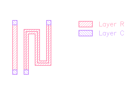
Resistor extractors (resistor and resistor_with_bulk)
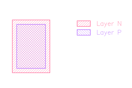
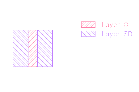
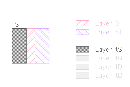
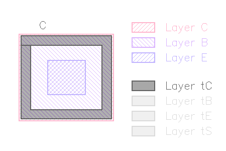
The resistor extractor assumes a layout which consists of a resistor "wire" and two caps (contacts). The wire is specified with the layer symbol "R", the caps are specified with the layer symbol "C":
The extractor will compute the resistance from the number of squares and the sheet resistance. The sheet resistance needs to be given when creating the extractor:
sheet_rho = 0.5
model_name = "RES"
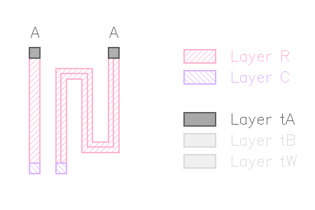
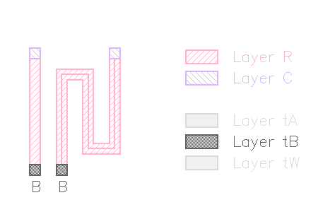
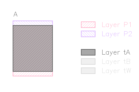
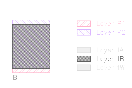
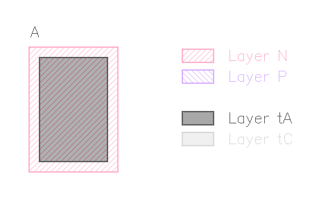
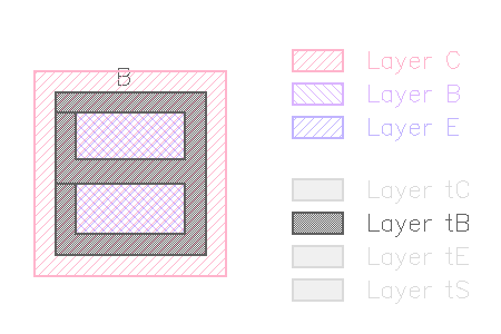
extract_devices(resistor(model_name, sheet_rho), { "R" => res_layer, "C" => contact_layer })The plain resistor offers two terminals which it outputs on "tA" and "tB" terminal layers. If "tA" or "tB" is not specified, "A" or "B" terminals will be written on the "C" layer. respectively.
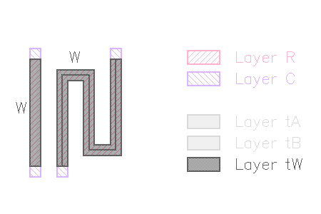
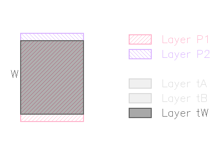
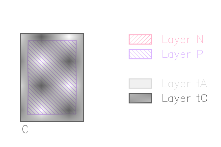
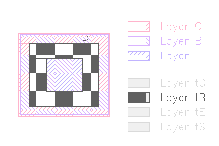
For the resistor with bulk, the wire area is output on the "tW" terminal layer as the "W" terminal:
Note: The resistance computation is based on a simple approximation. It computes the number of squares by tracing the perimeter of the "R" polygon. The perimeter length is separated in parts where the perimeter touches the "C" layer and parts where it does not. The number of squares is computed from the non-touching length divided by the touching length.
Capacitor extractors (capacitor and capacitor_with_bulk)
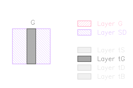
Capacitors are assumed to consist of two "plates" (vertical capacitors). The plates are on layers P1 and P2. The capacitor is extracted from the area where these two layers overlap.
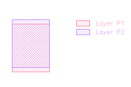
The extractor will compute the capacitance from the area of the overlap and the capacitance per area (F/µm²) value.
area_cap = 1.5e-15
model_name = "CAP"
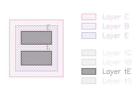
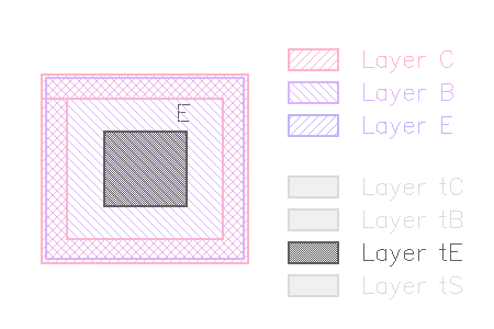
extract_devices(capacitor(model_name, area_cap), { "P1" => metal1, "P2" => metal2 })The plain capacitor offers two terminals which it outputs on "tA" and "tB" terminal layers. If "tA" or "tB" is not specified, "A" or "B" terminals will be written on the "P1" and "P2" layers respectively.
For the capacitor with bulk, the capacitor area is output on the "tW" terminal layer as the "W" terminal:
Diode extractor (diode)
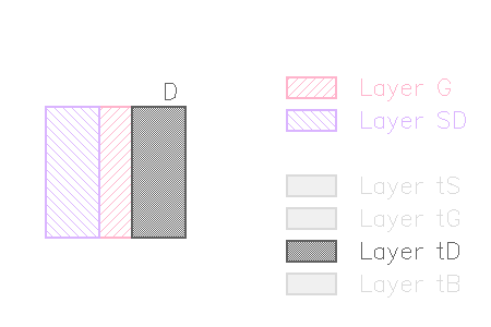
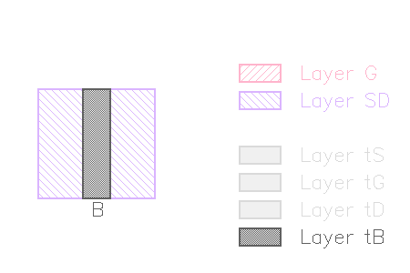
Diodes are assumed to consist of two vertical implant regions (wells, diffusion). One of the regions is p type ("P" layer) and the other "n" type ("N" layer). These layers also form the anode (p) and cathode (n) of the diode.
model_name = "DIODE"
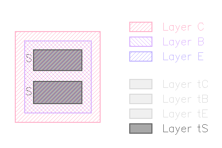
extract_devices(diode(model_name), { "P" => pplus, "N" => nwell })The diode offers two terminals which it outputs on "tA" and "tC" terminal layers. If "tA" is not specified, "A" terminals will be written on the "P" layer. If "tC" is not specified, "C" terminals will be written on the "N" layer.
MOS transistor extractor (mos3 and mos4)
MOS transistors are recognized by their gate ("G" input) and source/drain ("SD" input) regions. Source and drain needs to be separated from the gate shape. The touching edges of gate and source/drain regions define the width of the device, the perpendicular dimension the gate length. Because the separation of source/drain, the computation of gates and the separation of these for NMOS and PMOS devices, the "G" and "SD" layers are usually derived layers. As these usually won't participate in the connectivity, it's important to specify the "tS", "tD", "tG" and "tB" (for MOS4) layers explicitly and redirect the terminal shapes to layers that really participate in connections.
model_name = "PMOS"
extract_devices(mos4(model_name), { "SD" => (active - poly) & pplus, "G" => (active & poly), "W" => nwell,
                                    "tS" => active, "tD" => active, "tG" => poly, "tB" => nwell })
The MOS3 device produces three terminals which it outputs on "tS", "tG" and "tD" terminal layers (source, gate and drain respectively):
The MOS4 device offers one more terminal (bulk) which it writes on "tB".
Diffusion MOS transistor extractor (dmos3 and dmos4)
DMOS devices are basically identical to MOS devices, but for those source and drain are separated. This is often the case for diffusion MOS transistory, hence this name.
DMOS and MOS devices share the same device class. DMOS devices are configured such that source and drain cannot be swapped. The netlist compare will report source/drain swapping as errors for such devices.
DMOS transistors are recognized by their gate ("G" input), source ("S" input) and drain ("D" input) regions. Source and drain needs to be separated from the gate shape. The touching edges of gate and source/drain regions define the width of the device, the perpendicular dimension the gate length. The terminal output layers for DMOS devices are the same than for MOS devices: "tS" for source, "tD" for drain, "tG" for gate, "tB" for bulk (4-terminal version).
Bipolar transistor extractor (bjt3 and bjt4)
There are basically two kind of bipolar transistors: vertical and lateral ones.
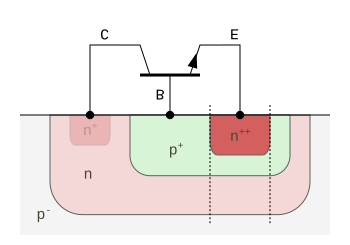
Lateral transistors are formed by implant or diffusion wells creating a intermittent n/p structure on the wafer. The basic recognition region is the base region. The collector and emitter regions are inside or overlapping the base region and use the opposite doping than base: if the base region is n doped, then collector and emitter regions have to be p doped. The structure then forms a PNP transistor. KLayout recognizes lateral transistors when the base is partially covered by the collector region. For lateral transistors, the emitter is defined by the emitter region inside base. The collector region is defined by collector inside base and outside emitter.
 (lateral NPN transistor)
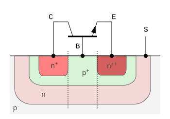
Vertical transistors are formed by a stack of n/p wells. Sometimes vertical transistors are formed as parasitic devices in standard CMOS processes. A PNP transistor can be formed by taking the collector as the substrate, nwell for the base and pplus implant for the emitter. KLayout recognizes a vertical bipolar transistor when the base is covered entirely by the collector or has no collector at all - this means the collector region can be empty (e.g. bulk).
 (vertical NPN transistor)
In both cases, there can be multiple emitter regions inside a base island. In this case, one transistor is extracted for each emitter region.
Vertical bipolar transistors
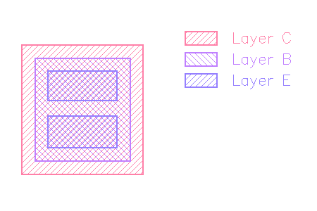
Vertical bipolar transistors take their inputs from "B" (base), "C" (collector) and "E" (emitter). "C" is optional:
Especially for bipolar devices it's important to device useful terminal output layers. Typically, the wells and diffusion areas will be connected through "contact", (not considering the Schottky diodes for now). So it's a good idea to send the terminals to the contact layer:
model_name = "PNP"
extract_devices(bjt3(model_name), { "C" => collector, "B" => base, "E" => emitter,
                                    "tC" => contact, "tB" => contact, "tE" => contact })
The BJT3 device produces three terminals which it outputs on "tC", "tB" and "tE" terminal layers (collector, base and emitter respectively):
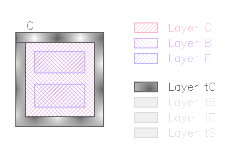
If the collector region is empty (e.g. p substrate), the base shape is copied to the "tC" output layer for the collector terminal.
The BJT4 device offers one more terminal (substrate) which it writes on "tS". "tS" is a copy of the emitter shape but connected to the substrate terminal:
Lateral bipolar transistors
Lateral bipolar transistors also take their inputs from "B" (base), "C" (collector) and "E" (emitter). For lateral transistors, "C" is not optional and must not fully cover the base region. Apart from this, the use model for BJT3 and BJT4 extractors is identical for vertical and lateral transistors.
A typical lateral transistor is formed by a collector ring and emitter island inside the base region:
The terminals produced by the bipolar transistor extractor in the lateral case are the same than for the vertical case, but with a different geometry:
Again, for BJT4, "tS" is a copy of the emitter shape but connected to the substrate terminal:
Device extractors and device classes
"extract_devices" will return the DeviceClass object of the devices generated. This object can be useful to apply some basic modifications. The most important of them is enabling or disabling certain parameters.
Most device extractors extract more parameters than they give you by default. For example, the resistor extractor will not just extract the resistance, but also the length (L) and width (W) of the resistor stripe and its area (A) and perimeter (P). By default these additional parameters are declared "secondary" - i.e. they will not participate in the device compare and will not be netlisted.
Parameters can be fully enabled by using enable_parameter or disabled using disable_parameter. tolerance can be used to enable a parameter for compare and to specify a compare tolerance. ignore_parameter can be used to ignore a parameter in the compare step.
Another way of customizing the built-in device extractors is to supply a custom device class. The following code creates a new resistor class which changes the preconfigured device parameter definitions to enable "W" and "L".
class MyResistor < RBA::DeviceClassResistor
  def initialize
    super
    enable_parameter("W", true)
    enable_parameter("L", true)
  end
end

...

extract_devices(resistor("RES", 1, MyResistor), ...)
Using a custom device class opens the option to supply additional parameters for example or to implement some entirely new device while using the extraction mechanics of the resistor extractor. The only requirement is compatibility of the parameter and terminal definitions.