LVS Introduction
LVS introduction
For introducing the LVS feature we consider the most simple CMOS structure there is: the two-transistor inverter.
Layout
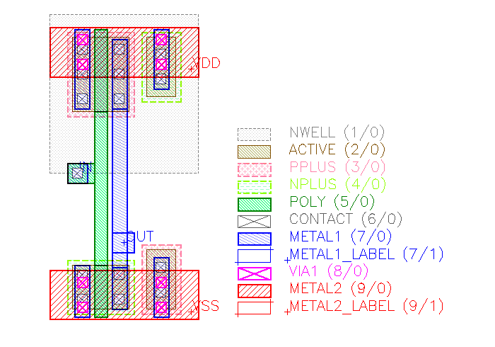
The inverter consists of two MOS transistors. A single transistor is made from an active region (a rectangle on the ACTIVE layer) and a gate (POLY layer) crossing the active region. The gate forms the channel from source to drain regions (left and right of gate). Contacts (CONTACT) provide connections from the first metal layer (METAL1) to the gate polysilicon (POLY) and to source/drain regions (where over ACTIVE). Via holes (VIA1) provide connections from the first (METAL1) to the second metal (METAL2). Finally, specific devices are formed by the source/drain implants which is n+ (NPLUS marker) for NMOS and p+ (PPLUS marker) for PMOS devices. PMOS devices sit in a n implant region (n-well) which forms the p-channel region. NMOS devices are built over substrate which is p doped to supply the n-channel region.
The actual layout is made as a standard cell. Multiple standard cells can be arrayed horizontally in a row. The power rails are formed in the second metal for VDD at the top and VSS at the bottom. The n-well extends over the top of the cell and is supposed to connect to neighbor well regions:

Schematic
For the inverter we can draw a schematic in a simplified form (left) and in a more realistic form (right) which also includes the bulk potentials of the transistors. It is important to keep the bulk of of the transistors at a defined potential to avoid latch-up. Hence we need pins for these terminals too. This makes a total of six pins: for input (IN) and output (OUT), for the power (VDD, VSS) and the two bulk potentials (NWELL, SUBSTRATE):

For LVS we first need a reference schematic. This is the SPICE netlist corresponding to the schematic with the bulk connections:
* Simple CMOS inverer circuit (inv.cir)
.SUBCKT INVERTER VSS IN OUT NWELL SUBSTRATE VDD
Mp VDD IN OUT NWELL     PMOS W=1.5U L=0.25U
Mn OUT IN VSS SUBSTRATE NMOS W=0.9U L=0.25U
.ENDS
The circuit we are going to analyze is a cell which is embedded in bigger circuits. Hence it makes sense to describe the inverter as a subcircuit. If the netlist consists of a subcircuit only, KLayout will consider this circuit. Otherwise it will consider the global definitions as the main circuit. In the latter case, pins cannot be defined while with subcircuits pins can be listed as given names too.
Sample LVS script
The LVS script to compare the layout above and the schematic now is this (for more details see LVS Reference):
# LVS script (demo technology, KLayout manual)

# Preamble:

deep

# Reports generated:

report_lvs     # LVS report window

# Drawing layers:

nwell       = input(1, 0)
active      = input(2, 0)
pplus       = input(3, 0)
nplus       = input(4, 0)
poly        = input(5, 0)
contact     = input(6, 0)
metal1      = input(7, 0)
metal1_lbl  = labels(7, 1)
via1        = input(8, 0)
metal2      = input(9, 0)
metal2_lbl  = labels(9, 1)

# Bulk layer for terminal provisioning:

bulk        = polygon_layer

# Computed layers:

active_in_nwell       = active & nwell
pactive               = active_in_nwell & pplus
pgate                 = pactive & poly
psd                   = pactive - pgate

active_outside_nwell  = active - nwell
nactive               = active_outside_nwell & nplus
ngate                 = nactive & poly
nsd                   = nactive - ngate

# Device extraction

# PMOS transistor device extraction
extract_devices(mos4("PMOS"), { "SD" => psd, "G" => pgate, "W" => nwell,
                                "tS" => psd, "tD" => psd, "tG" => poly, "tW" => nwell })

# NMOS transistor device extraction
extract_devices(mos4("NMOS"), { "SD" => nsd, "G" => ngate, "W" => bulk,
                                "tS" => nsd, "tD" => nsd, "tG" => poly, "tW" => bulk })

# Define connectivity for netlist extraction

# Inter-layer
connect(psd,        contact)
connect(nsd,        contact)
connect(poly,       contact)
connect(contact,    metal1)
connect(metal1,     metal1_lbl)   # attaches labels
connect(metal1,     via1)
connect(via1,       metal2)
connect(metal2,     metal2_lbl)   # attaches labels

# Global
connect_global(bulk,  "SUBSTRATE")
connect_global(nwell, "NWELL")

# Compare section

schematic("inv.cir")

align              # flattens unpaired circuits
netlist.simplify   # removes floating nets, combines devices

compare
For trying this script, load the inverter layout from "testdata/lvs/inv.oas" (KLayout sources) and open the Macro Editor IDE (Tools/Macro Development). Create a new script in the LVS tab and paste the text from above. Then run the script. The LVS report browser will open and show everything in green. This indicates the compare was successful:

Anatomy of the LVS script
The first and important statement of a LVS script should be the "deep" switch which enables hierarchical mode. Without hierarchical mode, the netlist is produced without subcircuits. Such flat netlist are inefficient to compare and hard to debug. Hence we switch to hierarchical mode with the "deep" statement (see deep):
deep
We also instruct LVS to create a report and open it in the report browser once LVS has finished:
report_lvs
We can also write the report to a file if we want (see report_lvs):
report_lvs("inv.lvsdb")The next step is the declaration of the input layers:
nwell       = input(1, 0)
active      = input(2, 0)
pplus       = input(3, 0)
nplus       = input(4, 0)
poly        = input(5, 0)
contact     = input(6, 0)
metal1      = input(7, 0)
metal1_lbl  = labels(7, 1)
via1        = input(8, 0)
metal2      = input(9, 0)
metal2_lbl  = labels(9, 1)
"input" and "labels" are functions which pull layout layers from the layout source (the layout source is - as in DRC - usually the current layout). While "input" pulls all kind of shapes, "labels" will only pull texts. We use "labels" to pull labels for first metal from GDS layer 7, datatype 1 and labels for second metal from GDS layer 9, datatype 1. For details see input and labels.
In addition, we create an empty layer which we will need to represent the "substrate". This layer does not constitute a closed region but rather a heap of shapes which will all connect to the same (global) net later:
bulk = polygon_layer
The names we give to the layers are actually variables which represent a layout layer. As in DRC, we can use these to compute some derived layers:
active_in_nwell       = active & nwell
pactive               = active_in_nwell & pplus
pgate                 = pactive & poly
psd                   = pactive - pgate

active_outside_nwell  = active - nwell
nactive               = active_outside_nwell & nplus
ngate                 = nactive & poly
nsd                   = nactive - ngate
These formulas are all boolean operations. "&" is the boolean AND operation and "-" is the boolean NOT. Hence "active_in_nwell" is the part of "ACTIVE" which is inside "NWELL" while "active_outside_nwell" is the part of "ACTIVE" outside it. The main purpose of these formulas is to separate source and drain regions but cutting away the gate area from the "ACTIVE" area. This renders "psd" and "nsd" (PMOS and NMOS source/drain). The boolean operations are part of the DRC feature set. For more functions and detailed descriptions see DRC Reference: Layer Object.
We also separate gate regions for PMOS (pgate) and NMOS transistors (ngate) and with these ingredients we are ready to move to device extraction:
extract_devices(mos4("PMOS"), { "SD" => psd, "G" => pgate, "W" => nwell,
                                "tS" => psd, "tD" => psd, "tG" => poly, "tW" => nwell })
The first argument of "extract_devices" (see extract_devices) is the device extractor. The device extractor is an object responsible for the actual extraction of a certain device type. In our case the template is "MOS4" and we want to produce a new class of devices called "PMOS". mos4("PMOS") will create a new device extractor which produces devices of "MOS4" kind with class name "PMOS".
The second argument is a hash of layer symbols and layers. Each device extractor type defines a specific set of layer symbols. For all devices, two sets of the layers are required: the input layers which the extractor employs to recognize the device and the terminal connection layers which the extractor uses to place "magic" terminal shapes on. These polygons will create connections to the devices produced by the extractor.
The input layers are designated by upper-case letters, while the terminal output layers are designated with a lower-case "t" followed by the terminal name. The specification above is complete, but because "tW" defaults to "W" and "tS" and "tD" default to "SD", it can be written shorter as:
extract_devices(mos4("PMOS"), { "SD" => psd, "G" => pgate, "W" => nwell, "tG" => poly })We also need an extractor for the "NMOS" class. It's built exactly the same way than the PMOS extractor:
extract_devices(mos4("NMOS"), { "SD" => nsd, "G" => ngate, "W" => bulk,
                                "tS" => nsd, "tD" => nsd, "tG" => poly, "tW" => bulk })
Having the devices is already half the work. We now need to supply the connectivity (see connect):
connect(psd,        contact)
connect(nsd,        contact)
connect(poly,       contact)
connect(contact,    metal1)
connect(metal1,     metal1_lbl)   # attaches labels
connect(metal1,     via1)
connect(via1,       metal2)
connect(metal2,     metal2_lbl)   # attaches labels
These statements will connect PMOS source/drain regions (psd) with CONTACT regions (contact), NMOS source/drain regions (nsd) also with CONTACT. POLY will also connect to CONTACT. Remember that we specified psd, nsd and poly as terminal outputs "tS", "TD" and "tG" in the device extraction. By including these layers into the connectivity, we establish device terminal connections to the nets formed by these layers.
The metal stack is trivial (CONTACT to METAL1, METAL1 to METAL2 via VIA1). The labels are attached to nets simply by including the label layers into the connectivity. The net extractor will pull the text strings from these connected text objects and assign them to the nets as net names.
Furthermore, two special connections need to be made (see connect_global):
connect_global(bulk,  "SUBSTRATE")
connect_global(nwell, "NWELL")
Global connections basically say that all shapes on a certain layer belong to the same net - even if they do not touch - and this net is always shared between circuits and subcircuits. This is certainly true for the bulk layer, but not necessarily for the NWELL layer. Isolated NWELL patches do not connect together. We will correct this small error later when it comes to extraction with tie-down diodes.
We have now provided all the essential inputs for the netlist formation. We now have to specify the reference netlist:
schematic("inv.cir")Two optional, but recommended steps are hierarchy alignment and extracted netlist simplification:
align              # flattens unpaired circuits
netlist.simplify   # removes floating nets, combines devices
"align" will remove circuits which are not present in the other netlist by integrating their content into the parent cell. This will remove auxiliary cells which are usually present in a layout but don't map to a schematic cell (e.g. device PCells). "netlist.simplify" reduces the netlist by floating nets, performs device combination (e.g. fingered transistors). This method will also create pins from labeled nets in the top level circuit.
The order should be "align", then "netlist.simplify". Both have to happen before "compare" to be effective. "align" is described in LVS Compare, "netlist.simplify" in LVS Netlist Tweaks.
Finally after having set this up, we can trigger the compare step:
compare
If we insert a netlist write statement (see target_netlist) at the beginning of the script, we can obtain a SPICE version of the extracted netlist:
# SPICE output statement (insert at beginning of script):
target_netlist("inv_extracted.cir", write_spice, "Extracted by KLayout")
Since we have a LVS match, the extracted netlist is pretty much the same than the reference netlist, but enhanced by some geometrical parameters such as source and drain area and perimeter:
* Extracted by KLayout

* cell INVERTER
.SUBCKT INVERTER
* net 1 IN
* net 2 VSS
* net 3 VDD
* net 4 OUT
* net 5 NWELL
* net 6 SUBSTRATE
* device instance $1 r0 *1 1.025,4.95 PMOS
M$1 3 1 4 5 PMOS L=0.25U W=1.5U AS=0.675P AD=0.675P PS=3.9U PD=3.9U
* device instance $2 r0 *1 1.025,0.65 NMOS
M$2 2 1 4 6 NMOS L=0.25U W=0.9U AS=0.405P AD=0.405P PS=2.7U PD=2.7U
.ENDS INVERTER
Inverter with tie-down diodes
The inverter cell above is not useful by itself as it lacks features to tie the n well and the substrate to a defined potential. This is achieved with tie-down diodes.
Tie-down diodes are contacts over active regions. The active regions are implanted p+ on the substrate and n+ within the n well (the opposite implant type of transistors). With this doping profile, the metal contact won't form a Schottky barrier to the Silicon bulk and behave like an ohmic contact. So in fact, the "diode" isn't a real diode in the sense of a rectifier.
The modified layout is this one:
The corresponding schematic is this:
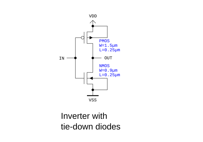
With this circuit, the n well is always at VDD potential and the substrate is tied at VSS:
* Simple CMOS inverer circuit
.SUBCKT INVERTER_WITH_DIODES VSS IN OUT VDD
Mp VDD IN OUT VDD PMOS W=1.5U L=0.25U
Mn OUT IN VSS VSS NMOS W=0.9U L=0.25U
.ENDS
The LVS script is slightly longer when extraction of tie-down diodes is included:
# LVS script (demo technology, KLayout manual)

# Preamble:

deep

# Reports generated:

report_lvs     # LVS report window

# Drawing layers:

nwell       = input(1, 0)
active      = input(2, 0)
pplus       = input(3, 0)
nplus       = input(4, 0)
poly        = input(5, 0)
contact     = input(6, 0)
metal1      = input(7, 0)
metal1_lbl  = labels(7, 1)
via1        = input(8, 0)
metal2      = input(9, 0)
metal2_lbl  = labels(9, 1)

# Bulk layer for terminal provisioning

bulk        = polygon_layer

# Computed layers

active_in_nwell       = active & nwell
pactive               = active_in_nwell & pplus
pgate                 = pactive & poly
psd                   = pactive - pgate
ntie                  = active_in_nwell & nplus

active_outside_nwell  = active - nwell
nactive               = active_outside_nwell & nplus
ngate                 = nactive & poly
nsd                   = nactive - ngate
ptie                  = active_outside_nwell & pplus

# Device extraction

# PMOS transistor device extraction
extract_devices(mos4("PMOS"), { "SD" => psd, "G" => pgate, "W" => nwell,
                                "tS" => psd, "tD" => psd, "tG" => poly, "tW" => nwell })

# NMOS transistor device extraction
extract_devices(mos4("NMOS"), { "SD" => nsd, "G" => ngate, "W" => bulk,
                                "tS" => nsd, "tD" => nsd, "tG" => poly, "tW" => bulk })

# Define connectivity for netlist extraction

# Inter-layer
connect(psd,        contact)
connect(nsd,        contact)
connect(poly,       contact)
connect(ntie,       contact)
connect(nwell,      ntie)
connect(ptie,       contact)
connect(contact,    metal1)
connect(metal1,     metal1_lbl)   # attaches labels
connect(metal1,     via1)
connect(via1,       metal2)
connect(metal2,     metal2_lbl)   # attaches labels

# Global
connect_global(bulk, "SUBSTRATE")
connect_global(ptie, "SUBSTRATE")

# Compare section

schematic("inv2.cir")

align
netlist.simplify

compare
The main difference is the computation of the regions for n tie-down (inside n well) and p tie-down. This is pretty straightforward:
ntie                  = active_in_nwell & nplus
ptie                  = active_outside_nwell & pplus
Device extraction does not change, but we need to include the tie-down regions into the connectivity:
connect(ntie,       contact)
connect(nwell,      ntie)
connect(ptie,       contact)
By connecting ntie to contact and nwell, we readily establish a connection to n well which behaves then like a conductive layer (although the resistance will be very high). Remember the the device extractors for PMOS will put the bulk terminals on nwell too, so the transistor is automatically connected to the nwell net.
ptie cannot be simply connected as there are no polygons for "substrate". But we can include ptie in the global connections:
connect_global(bulk, "SUBSTRATE")
connect_global(ptie, "SUBSTRATE")
nwell is no longer included in the global connections, hence we do no longer and incorrectly consider all nwell regions to be connected.
The extracted netlist shows the bulk terminals of NMOS and PMOS connected to source (drain and source are equivalent):
* Extracted by KLayout

* cell INVERTER_WITH_DIODES
.SUBCKT INVERTER_WITH_DIODES
* net 1 IN
* net 2 VDD
* net 3 OUT
* net 4 VSS
* device instance $1 r0 *1 1.025,4.95 PMOS
M$1 2 1 3 2 PMOS L=0.25U W=1.5U AS=0.675P AD=0.675P PS=3.9U PD=3.9U
* device instance $2 r0 *1 1.025,0.65 NMOS
M$2 4 1 3 4 NMOS L=0.25U W=0.9U AS=0.405P AD=0.405P PS=2.7U PD=2.7U
.ENDS INVERTER_WITH_DIODES