Howdy, Stranger!
It looks like you're new here. If you want to get involved, click one of these buttons!
Quick Links
LVS: check connection and resistance of multilayer via chain

Hello,
I asked the same question here https://github.com/KLayout/klayout/issues/929 and unfortunately didn't understand the answer.
So I would like to check the connection in so-called via chain structure to be sure that there are no opens (via or metal planes missing). I also would like to calculate the resistance of all layers (including vias).
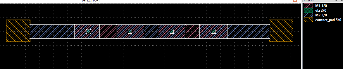
Roughly the schematics depicted below

I can't understand how to tell the resistance model that all layers are connected between each other. The connect function didn't work for me.
Comments
@anatolyb So you didn't mention that you are looking for the resistance of a periodic via chain. This is a typical yield or reliability test structure, not a resistor you would usually use in a design.
First of all you need a way to tell wiring from resistor "devices". Vias are usually used for providing the connection between two metals. These you don't want to extract as resistors. So you need some kind of marker layer which you draw over the via chain to mark this area.
But as @dick_freebird mentioned, you need to indicate how your resistance is computed: will this be dominated by the single via resistance (so proportional to the number of vias traversed) or is so you need to take into account the wire resistance too?
The final solution depends on this model. If the via resistance dominates, a potential solution is to extract single vias as resistors and let the netlist reducer join parallel and serial via "resistors" into the final one.
Matthias
In case you go for the "dominant via" solution and to provide an educational example for a custom device extractor, here is a solution.
The basic problem is that KLayout does not offer a "vertical resistor" by default, but we can add that type using a custom device extractor.
A sample layout is attached. It features two metals, a via and the discussed marker layer (4/0):
The corresponding LVS script is this:
The script lacks the schematic input and compare steps, but it extracts and displays (because of "report_netlist") and netlist.
Small disclaimer: the "combine_devices" step will join all via "resistors" even if they belong to different "islands", like here:
A solution to this problem is to put the "islands" into separate child cells.
If you need a more elaborate solution, you can essentially consider everything inside a single marker "island" one device, pull all the shapes into the device extractor and code the via chain assembly and resistor computation yourself. But I think that is not an easy task to code.
Matthias