Howdy, Stranger!
It looks like you're new here. If you want to get involved, click one of these buttons!
Quick Links
Net connection identify with wide dielectric opening

Hello Matthias:
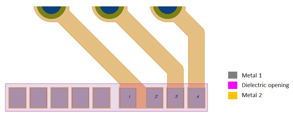
I assume the logic to judge connection nets is by pattern touching or not between up/down layers, please check attached image. Somehow the dielectric opening will be designed as a wide region as below pink area. If so, net connect function will identify net [ 1, 2, 3, 4 ] as connected , but actually just #1 & #2 is one group, #3 , #4 are individually stand, not sure there is a better way to sort them ? I am trying to achieve this, will post when overcome it, thanks.
Comments
Not only will they be connected, but this layout would violate
basic layout rules. Specifically, via must stop on metal below,
else you will etch further into lower interlevel / field dielectric.
You will have a fight on your hands, when you get to foundry
tape-in DRCs as this rule I have never seen waived.
I guess this is more like PCB layout?
Dielectric opening in VLSI is typically a patch smaller than metal and it's a metal-filled plug that connects metal sheets - hence is conductive. I guess in your case, "dielectric opening" is where the isolation layer is missing and metal1 and metal2 touch. This is kind of different what VLSI metal stacks do.
Still you can emulate this technology flavour by using booleans:
Matthias
I am sure that you are expert in VLSI
Yes, this design is belong to post-VLSI field, and connect( metal, " via ", metal ) is not available in this application, but it is ok to embed intersection method as Matthias provided if any wide dielectric opening be placed.
Klayout save my life
Sorry, an accident..
I take it that these are "post fab" RDL features, then?
I worked at an RFIC company for a while, they used RDL
copper for some products. The CAD group had to add these
layers to the basic foundry layer set in order that the
designers could verify against the schematics which had
to incorporate the RDL features (inductors as well as
basic connectivity).
No reason you couldn't do the same (if you had the front
end PDK in hand).
The post-fab processing had its own rules, and you might
want to pay attention to process details in the case that the
post-fab processing includes an etch chemistry which could
attack normal pasivation (i.e. if your "dielectric opening" is
formed by an etch of the same chemistry as your foundry
pad opening, watch out for the "stops on" (leading to must-
surround).
If the dielectric is polyimide or something like that you're
probably OK. But if it's a deposited glass or nitride, take
care.
@dick_freebird
Hello, thanks for sharing the experience. At my site, polyimide is common material to do electric isolation, and wet etching is usually performed, special chemical with high etching selectivity ratio, means even no FAB material will be consumed.
I think LVS is more easier in package level, this case already be solved by the boolean "AND" with simple NetTracerTechnology method. LVS of VLSI super interests me, now I just start to learn, thank you.