Howdy, Stranger!
It looks like you're new here. If you want to get involved, click one of these buttons!
Quick Links
Path Check and repair

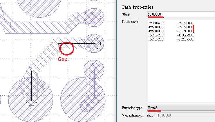
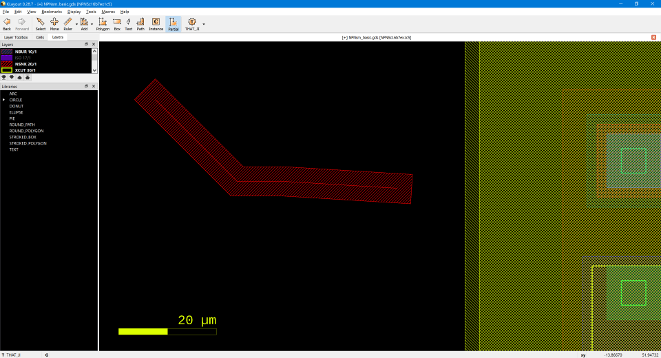
Hi sir ,
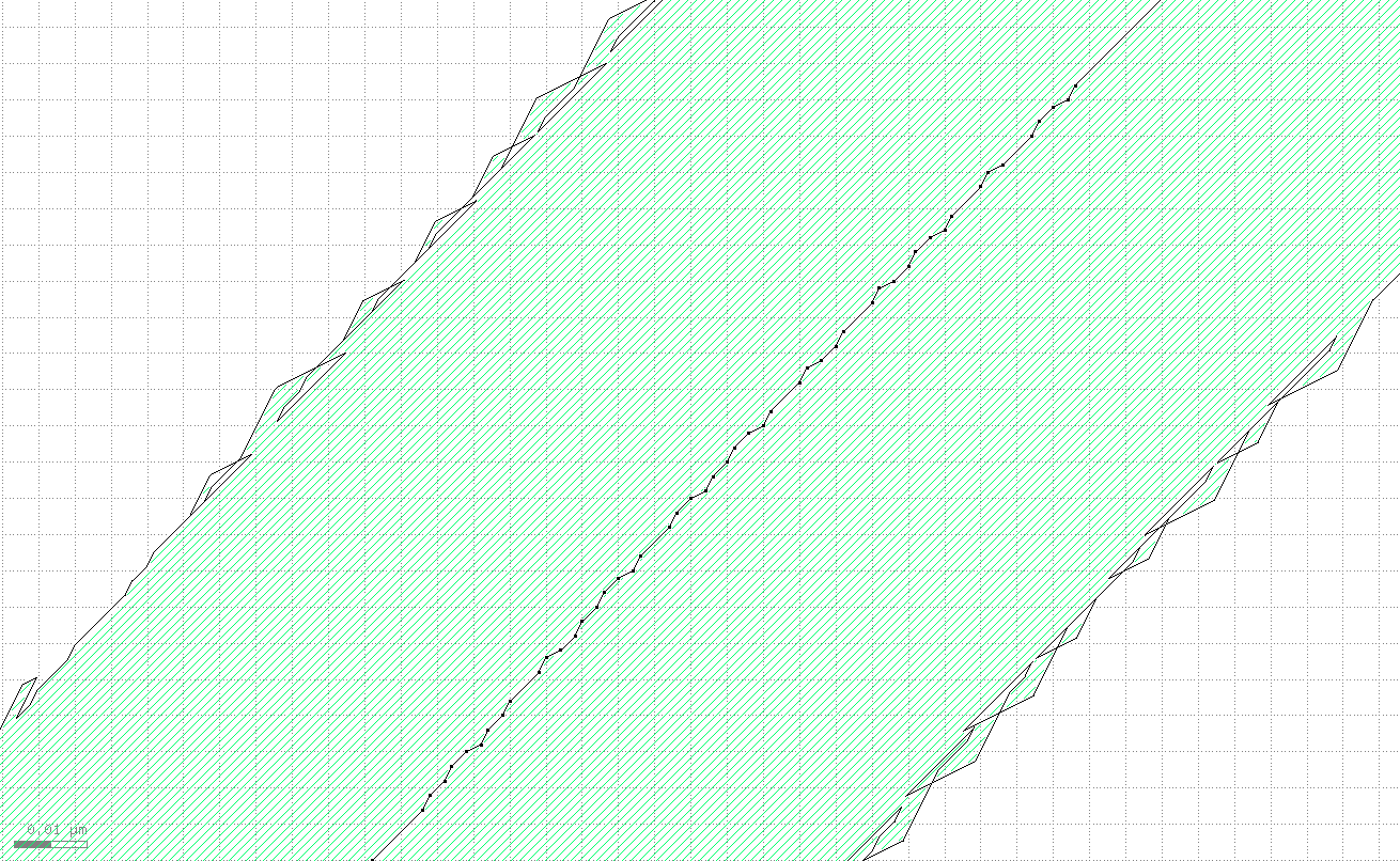
as Picture showning , I want to check /fix this path issue , that will make a gap in the area.
in the DRC function , can I check path points and width ?
(in the area , we have a lot of pattern , include shape and path , I need a function to filter path/shape in first.
Comments
The only way I fix these is by overlaying a "filler" or "cutter"
polygon and doing a merge or subtract as appropriate.
I imagine that Partial could drag the path straight too.
You have some other, uglier ones to fix around the round
pad at lower right and that needs something else.
Hi jiunnweiyeh
I think DRC will turn all the shapes in to polygons or edge pairs, which at that stage the engine can no longer distinguish betwee a path and a shape object.
by using KLayout API we can easily filter out path objects and check for small segments individually.
this example only check path segment length and without considering small gaps formed by pattern stacking and intersecting.
Hi jiunnweiyeh
if you don't care what causes the small gap and just want a fixed and get a gap-free version of the layer
you can try to utilize the size up and down function to eliminate gaps and output to a separate layer for tape out.
and this can be achieved with just one line of code.
Hi Rawr,
Thanks for your coding.
in my case , the design path been provided by customer and look like they using other design tool,
for draw / design the connect path.
it is reason our designer find that in some of our case.
when I check the path gap location , I find that may a solution to fix what the case I face to currently.
here is my code , I just remove the path segment when the length small than width /8.0
Actually, I have no idea for why that can fix trace/path broken issue , I just try and error base on
my coding capbility...
Hi jiunnweiyeh
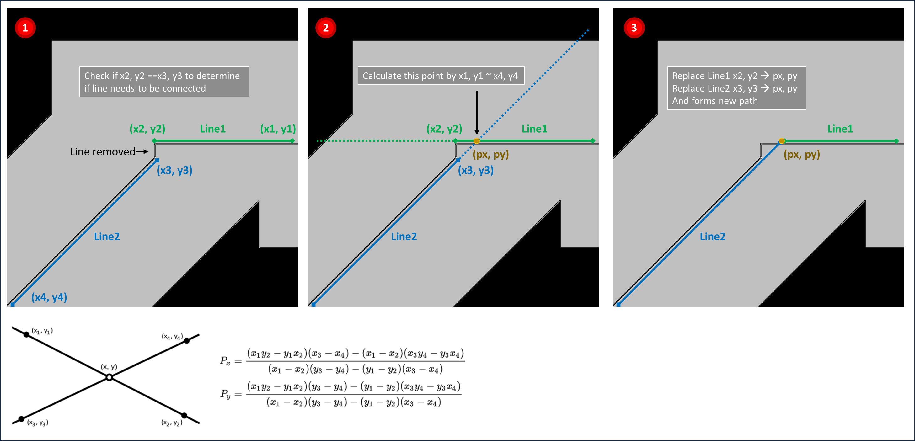
It's me again, I've adapt your method and do some modification, the change I made is adding a new point at where small line segment is being removed.
the purpose of this it to keep all the lines at it original place and avoid having lines that is at a wierd angle.
the process for adding points, for the calculation please refer to this page
https://en.wikipedia.org/wiki/Line–line_intersection
Dear all,
many thanks for this discussion and the nice contributions.
In general, the problem arises when path segments are shorter than the half-width of the path. This is a situation that should be avoided for well-formed paths (some foundries have respective design rules).
In your case with the round-ended paths, the usual way of fixing such issues is to resolve paths into sequences of round-ended segments, similar to what the circular aperture in Gerber does. Such a function is not readily available, but it can be scripted:
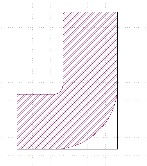
Here is the effect (red: after, blue: before):
the takeout shows how the resulting overlay paths become smooth:
In the PCB/Gerber world, the smooth edge transition following a circular contour is desired, while this is not the case in the VLSI world that KLayout stems from. In this world with Manhattan-style layouts, the corner-edge stitching mode is the commonly accepted behavior and round-ended paths are a legacy concept that usually is avoided.
Matthias
Hi Rawr / Matthias ,
Got it , Thanks very much for all your share.
I will try my best to review my coding base on your recommend.
I knew some part of my code is odd(stange) , that is what result base on try and error in my side.
some of code didn't have many Math principle / logic , I have to learn more and more.
Thanks your help.
Hi Rawr,") ,
,
some of case in your code.. the "((x1 - x2) * (y3 - y4) - (y1 - y2) * (x3 - x4))" will be zero (0)
I still under try to find other solution
Hi jiunnweiyeh
the case that triggers this error is when we tried to find an intersection point of two parallel segments
I've modified the condition for connecting broken sections
if the line is not connected, check the slope and create an intersection point of is a non-parallel line orjust reconnect them if is parallel line
Hi guys,
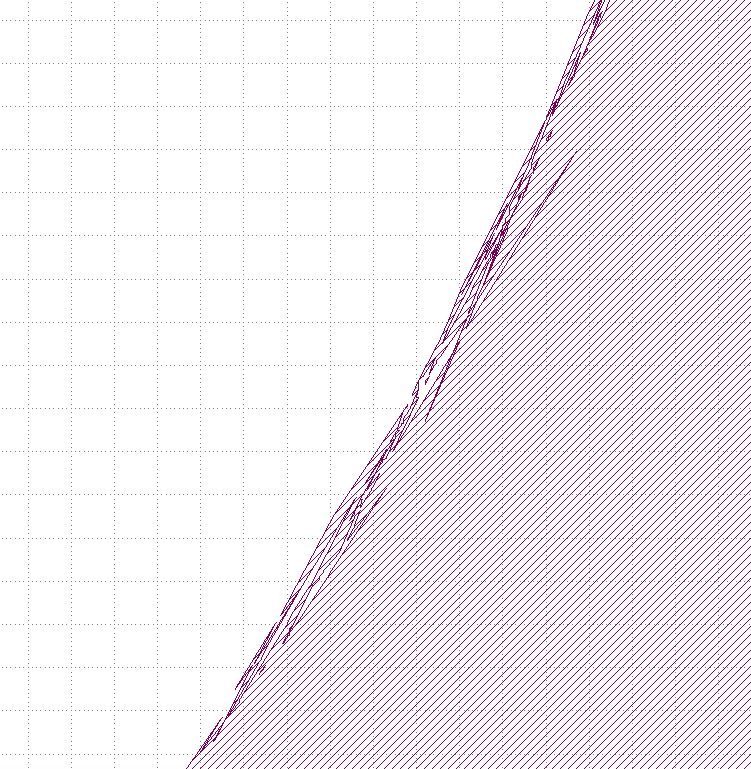
I am an student learning optoelectronic chip layout , Sometimes I have a problem which electrical chip won't have. For example
I write a function to generate Points ,then use Path.new([Points],width) to draw a waveguide .Here comes a question: A waveguide have a turn, and the turn radius is small, but the waveguide width is relatively big ,
then the Polygon drawn is not correct
As you can see, Its edge is a mess. I think it's the fault points order makes the mess. If I make the spacing between points larger , the mess disappered, But the accuracy will not be enough.
This problem has been bothering me all along, Anyone have a good idea to solve this?
Hi Default
if you check the path segment by segment like the image show below, you'll observe colsely you'll see that the path is actually doing a quite sharp turn and causing the edge portion swinging back and forth and results in a broken edge contour
follow (0) red --> (1) orange --> (2) yellow --> (3) green --> ...
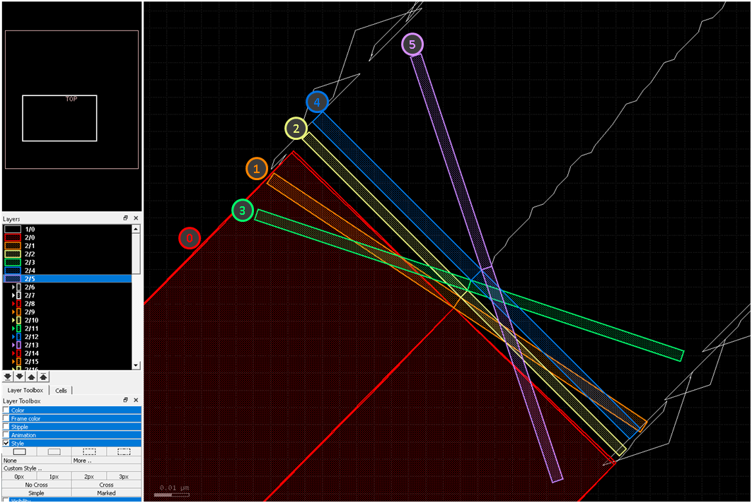
To elimitate this the segment length needs to be increased and the angle of each turn needs to be reduced.
and to have a more accurate control of each turn angle, you might need to adjust to a even finer grid size.
another way is to adopt Matthias approach and replace path into a round edge segments.
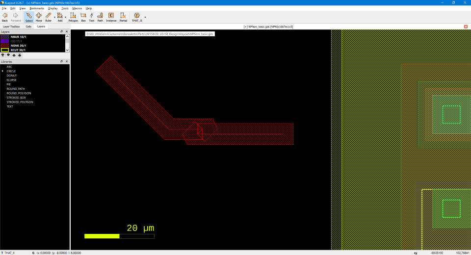
Just a thought, but to me looks like there are too many vertices
and some make for kooky path generation.
Is it practical to use Partial to select one "don't need" vertex and
delete it? This seems to work for me, deleting a vertex leaves the
rest and the path regenerates with one less segment.
Messy path:
Partial select one vertex:
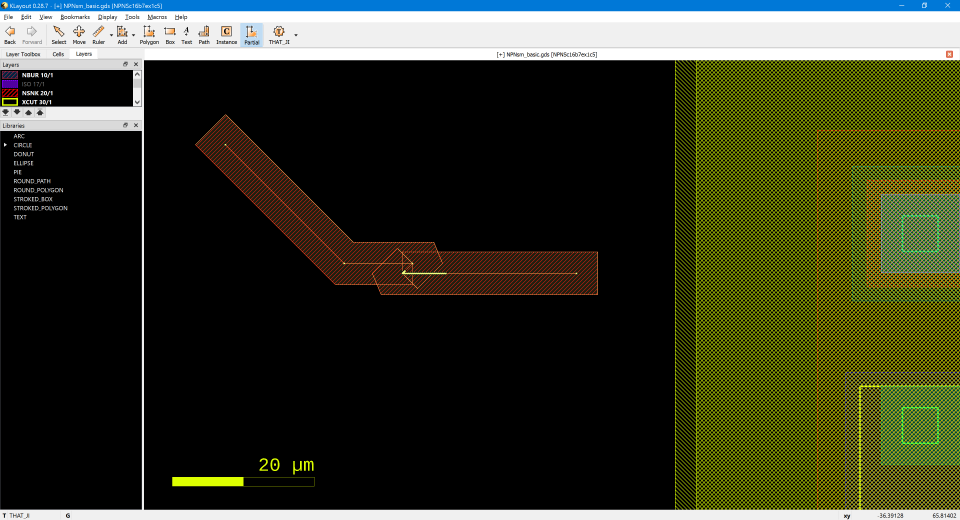
After Delete, one less vertex, still a path:
I imagine this could be somehow scriptable, to find (say) a vertex
which lies between two segments which have "abnormal" angles
(like, I would never make a <90 angle ever - I do 90 and "45s"
which are really 135 degree, acute angles will always make a
DRC space / notch error that has to be papered over in the sub-rule
gap region.
Hi All,
In my view , cause we (bumping house) didn't design RDL (path routing) by our side.
Our customer make that by them and maybe using Candence APD or other EDA tool to make path routing.
They just transfer routing file from candence format (mcm/sip) to GDS directly.
It is why we will face to this issue and need a way to fix it---the routing is been designed by customer.
and many DRC check result when we do rule check.
I have to try to find a solution to repair(fix) that because it have rule issue.
But , I never find the path pattern as Default 's sample in previosuly case.
In currently , Rawr / Matthias 's script can help me to fix that issue (almost) ,
some of that still need our designer to modify by manufature.
But , our customer have another question---Can we only fix (re-path) what the issue path and keep original shape of others path if it is fine?")
I am try to make a script to process it , maybe a space or degree check first for that.
anyway , Thanks all of your help
As a practical and business-protection matter, you should have
published a set of layout groundrules which your RDL process
can manufacture, and insist that a customer DB run clean to
some agreed-upon design rules check.
If you did your part and they did not do theirs, then kick it back
for rework and reverification.
If you touch it, then whatever happens becomes your fault
(unless you get the customer to sign off and make sure no
loopholes are left, because customers can turn into whiney
litigous bitches as soon as it costs them anything). Your
paperwork should be crafted such that they will do their
damn job rather than try to stuff bad data down your production
line so they can claim tapeout-on-time.
Of course this has nothing at all to do with CAD, but more
"CAD politics".
Hi @RawrRanger ,
Thanks for your help! Now I use a new method:
Draw this path with width=1(dbu) and then sized that path to the width i need, then cut the head and tail redundant.