Howdy, Stranger!
It looks like you're new here. If you want to get involved, click one of these buttons!
Quick Links
Remove cells outside polygon

Hello,
I am trying to automate my design process to remove specific cells outside of a polygon. Particularly, I am removing dummy pads outside a wafer exclusion zone.
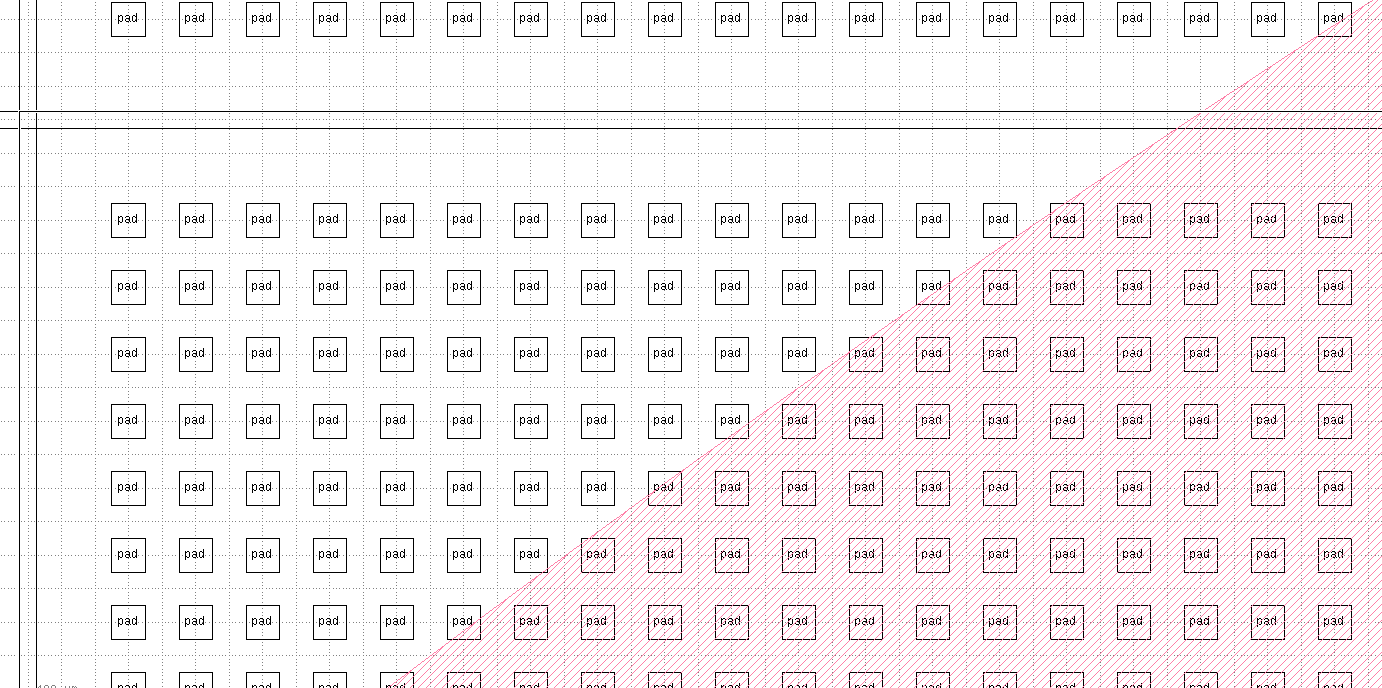
I have added two screenshots to help illustrate. I want to remove the 'pad' cells that are outside the red layer. If the pads are partially contacting the red layer, I could either remove all or leave them all, as long as it is consistent.
If someone could point me into the right direction that would be great! Please let me know if I need to explain better.
Thanks,
Dan
Comments
Another option could be removing all 'pad' cells that are greater than a set distance from the center of the design.
I am open to any practical solution. If anyone could set me on the right path, that would be great. I have limited coding skills but am open to learning so I can write it myself.
Hi Dan,
there are some solutions, but they depend on your requirements:
If the layout can be flattened (at least this layer), the DRC's "interact" or "inside" method will give you only the shapes inside the boundary polygon. The layer will become a sea of polygons then. This takes more memory, but if it's just pads, the effort should be manageable. Use tiling mode in DRC for a better memory performance.
If your cells are single instances (not AREF's), they can probably be removed by some script. But I assume these cells are placed inside another hierarchy (the chip), so the chip needs to be resolved - otherwise the pads will be removed in other instances of the chip too. That basically leads to the same approach than 1.) but will cell instances instead of polygons. I don't think there is much gained.
If your cells are AREF's they need to be resolved into single instances. Back to 2.)
So bottom line is, I'd try the DRC approach as the lowest hanging fruit.
Kind regards,
Matthias
Hi Matthais,
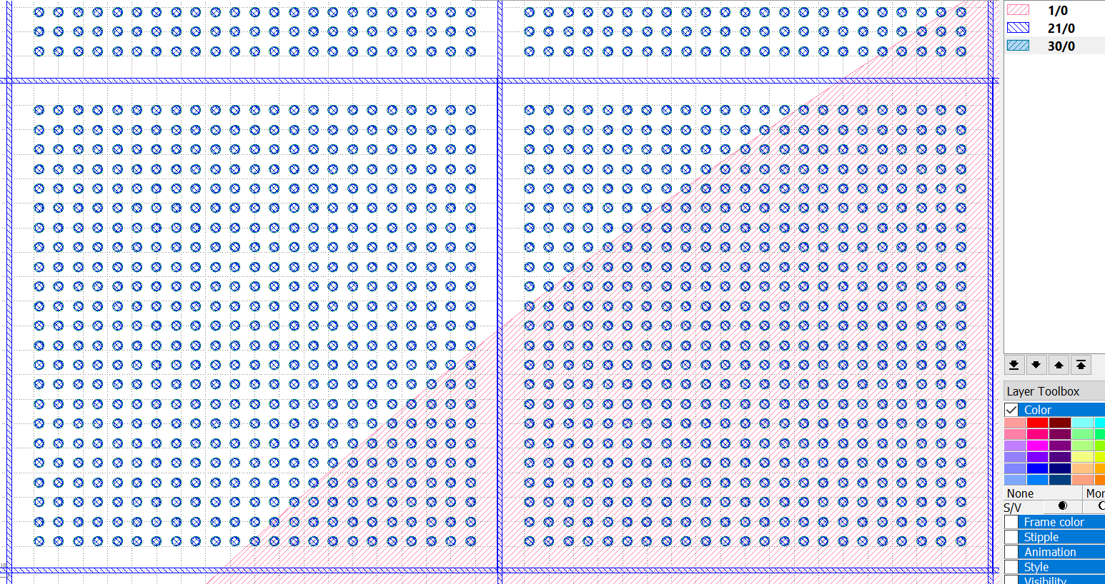
Thanks for the help and insight. I do not want to flatten the pads, so I can edit them latter if needed. You're correct, the pads are in another hierarchy (see screenshot). I do not want to flatten the die if it is not being changed.
Here is what I think would work-
Selectively flatten die and resolve pad array if any part is outside the polygon
Remove any pad cell that is outside the polygon.
Do you think this is possible and/or worthwhile to try and do?
Thanks,
Dan
Hi Dan,
I think this is feasible but the details depend on the nature of your layout. Maybe you can submit a sample file here?
Thanks,
Matthias
Hi Matthias,
I have added an example layout. Generally, we will have a flattened outline of the wafer (shown as layer 1). We are trying to clear all 'pad' cells that are outside of the this layer (or greater than a set distance from the center). The attached file has a simplistic hierarchy, but the pad cell we want to remove is usually 2-3 instances down from the top, e.g. Wafer>reticle>die>pad. The pads are in an array, but that is not necessary.
Please let me know if you have any other questions or concerns. Look forward to hearing you thoughts on how to solve this problem.
Thanks,
Dan
Hi Dan,
I'm sorry, but I don't see an attachment :-(
Did I miss anything?
The forum only accepts know formats - you'll need to zip a GDS file if you want to attach it.
Thanks,
Matthias
Hello Matthias,
I have the exact same query, but maybe I can simplify the background. In my case, I have flattened the hierarchy and resolved the array in such a way that my individual DIE cells are in the same Top Cell as the Bounding Polygon.
I have been thinking of two alternatives, but I cannot seem to find a way ahead in either:
1. Selecting the cells that lie outside the bounding polygon and then deleting them.
2. Creating a polygon outside the bounding region, so that the cells to be deleted lie within this second polygon.
In either case, I suppose an additional cleanup along the edges would be required, but that would still be a lot less cumbersome than having to clear out hundreds of other instances manually.
Thanks and regards,
Advait
Hi Aadoo/Dgrichte ...
I guss you want to remove some of "pad" cell outside of wafer edge. (300mm?)
here is methon what I do by manual...
1.check the cell "die" out of 300mm edge.
2.flattern 1 or 2 level , to make the "pad" cell in current cell view..
3.check the "pad" cells , if that is outside 300mm edge. remove it.
But , I am sorry , I can't make it as a script code for that.
hope my explain is correct and helpful for someone to do tht coding.
Hi jiunnweiyeh
Thanks for your message, this method is what I am following already. As I mentioned, the problem is that there are several hundreds of such cell instances that have to be removed, and you can check only a certain rectangular box of cells at a time with multiselect. While it works well, it is still very time-consuming, and therefore I (probably dgrichte too) wish to have a scripting alternative.
Regards
Advait
Hello,
For a circular "wafer" region it is very easy: just check the distance of the "bump" cell instance origins.
The code below only works if the "bump" cell instances are on the top level (if not, you can add some code to flatten some levels first (and even delete cell instances with a specific name only), but this depends on your design hierarchy). The "bump" should preferably be centered inside the "bump" cell.
module MyMacro
include RBA
end # MyMacro
before: "bump" cell instances at top level
after: "bumps" deleted outside wafer area (in the example a mini-wafer of 1000um ;.)
Cheers,
Tomas
@tomas2004 Thanks for the code!
In a different post I have mentioned a general rule to not delete anything while iterating. In this case it works as deleting the instances has a linear effect on the list we're iterating over, at least in editor mode.
However, this may not work in viewer mode. So to emphasize the general rule of iterate-then-delete, I'd like to propose this modification:
Best regards,
Matthias
Hello Tomas and Matthias,
many many thanks for this. I tried it out and it works exactly as I wanted. There is a little cleanup required for the instances that lie partially inside/outside, but it's much easier of a task than before.
Best regards
Advait
Hi Advait,
You can make the "wafer_size" variable slightly smaller than the exact wafer size to avoid bumps being placed on top of the physical wafer edge... Or add an additional variable "offset_from_wafer_edge" and then use "wafer_size/2.0 - offset_from_wafer_edge"...
Cheers,
Tomas
Hi Matthias,
Thanks for the tip and the great support!!! I learned so much from you...👍
Cheers,
Tomas
Hi Tomas,
I modified the wafer size on the basis of edge exclusion, but the thing is, the instance_distance formula utilizes the coordinates of the point of instantiation and not the size of the object within. Therefore it leaves behind cell instances that are instantiated within the inclusion boundary, but extend over that limit w.r.t. size. An example would be the 6th row from the center line in your image.
While writing this very reply however, I found a way and modified Matthias' code as follows (my instance cell structure has rectangular dimensions of 400x200 centered at origin):
I do not know if this is the appropriate way, but it worked. The only thing I would now need is for the macro to extract the instance dimensions directly and insert in place of 400 and 200, so that it becomes generalized for any dimensions.
Thanks a lot and best regards
Advait
Hi Advait,
instance.dbbox.height and instance.dbbox.width wil give you the height and width of the instance in microns...
Cheers,
Tomas
Hi Tomas,
Excellent! This takes off a lot of load off me.
Thanks a lot again and cheers!
Advait
Hi Matthias,
Here was my code , I have another request , almost like the code you provided.
if the cell instance location , out of wafer_size (300000.0) , I want to replace that as "DymmyDIE" cell.
that is a cell I have prepart .
Could you please help to confirm how to do that ? look like I can't using the code below...
Thanks.
Hi,
You just have to make these instances refer to your "DummyDIE" cell...
Cheers,
Tomas
Hi Tomas,
Thanks for your help , do you have idea for how to resolve array ?
instance.explode
Hi Tomas,
Thanks for your answer , I will try it.
Hi all,
One remark from my side: when you change a collected while you iterate over it, the behaviour is not defined. As "instance.explode" generates new instances, this is the case when you put this call into the loop.
A safe scheme in general is to collect the instances in question and then modify them:
Matthias
I want to go back to the original question-
if it is a particular shape of a layer (not circle necessarily), can instances (after explode) be deleted which are outside the shape without flattening it.
You can take the code from July 2021 and modify the filter criterion. You can check a instance bounding box vs. a filter polygon for example using
Polygon#touches(box).Matthias
I am still interested to see a "select mask" capability based on a
layer / polygon.
My thinkiing goes to the old Cadence behavior (seemingly broken
in IC6 layout, but remaining in schematic / symbol editors) that
keyed on the instance/drawing layer so define a "selectable
region" of a drawing (layout, symbol) instance. Click inside and
you get it, outside (but within extents) and you don't.
This is -way- handy for complex analog layouts where block
extents may overlap (or multiple, of) and a well defined
target is very helpful to constrain false-selects.
But a complementary function, that -prevents- selection of
instances within / below, I could also see being useful.
I'd propose a couple of setup fields that define the "select inside"
layer (default to instance / drawing, mapped to GDS layer/purpose)
and "select outside" (probably no default, but part of technology
layers set I'd guess) and logic about who overrides whom (I'd say
this could be "select outside" active only at present level, defeats
the default "select inside" of placed objects at that same present
level) and lower levels are ignored.
I want my "instance box"!
Hi,
You can run the script below after specifying the following variables:
instance_region_layer = "2/0"
regional_layer_sizing = 0.01
touching = false
resolve_arrays = true
I've also attached a small gds test case.
I would not use it for filling, as the built-in "Fill Tool" utility will work much faster, but it can be used for wafer mapping, wafer bumping, ...
Cheers,
Tomas