Howdy, Stranger!
It looks like you're new here. If you want to get involved, click one of these buttons!
Quick Links
Connectivity Based Stamping check

Hi @Matthias,
Thanks for this great tool. It's amazing and really comprehensive. We are trying to develop a DRC rule deck and we are faced with a rule the basically doesn't allow certain transistors in specific layer to have different connections. Basically, you could have one transistor only in each polygon. If you have multiple transistors you have to connect them in parallel or in series so effectively they are one transistor at the end. The problem with such check it depends mainly on connectivity.
Looking at what you posted here:
https://www.klayout.de/forum/discussion/1371/drc-nwell-spacing-with-same-different-potential
We came up with some similar code and ideas. But now we are facing a problem with ruby code. It doesn't allow adding objects to an array. Or may be there is a better way you might think of to do this check.
I have made up a technology and layer names here:
pdiff 1/0
poly 2/0
nwell 3/0
cont 4/0
metal1 5/0
And Here is the code that we have developed:
report("out")

def check_stamping(stamped_layer, stamping_layer, dev_layer)

  good_sd = polygon_layer

  stamped_layer.data.each do |p|

    single_polygon_stamp = polygon_layer
    single_polygon_stamp.data.insert(p)

    #stamp_in_polygon = stamping_layer & single_polygon_stamp
    dev_in_polygon = dev_layer & single_polygon_stamp

    net_devices_array = Array.new

    dev_in_polygon.data.each do |in_dev|
      single_dev_layer = polygon_layer
      single_dev_layer.data.insert(in_dev)

      dev_nets_array = Array.new
      stamp_in_dev = stamping_layer & single_dev_layer

      stamp_in_dev.data.each do |s_dev|
        curr_point = nil
        s_dev.each_edge do |e|
          curr_point = e.p1
          break
        end

        sd_net = l2n_data.probe_net(stamping_layer.data, curr_point)
        dev_nets_array.insert(sd_net)
        puts("Net name : ", sd_net.circuit, sd_net.cluster_id)
      end

      #net_devices_array.insert(dev_nets_array)
    end

    #net_devices_array.each_cons(2) do |a, b|
    #  puts(a)
    #  puts(b)

    #end
  end

  return good_sd
end


pdiff          = polygons(1, 0)
poly           = polygons(2, 0)
nwell          = polygons(3, 0)
cont           = polygons(4, 0)
metal1         = polygons(5, 0)


psd = (pdiff - poly) & nwell
pgate = poly.interacting(pdiff) & pdiff
fpoly = poly - pgate


connect(psd, cont)
connect(pgate, fpoly)
connect(fpoly, cont)
connect(cont, metal1)

netlist


possible_fail_stamp = nwell.interacting(psd, 3)
dev_layer = pdiff.inside(nwell).interacting(psd)
failed_stamp = check_stamping(possible_fail_stamp, psd, dev_layer)

possible_fail_stamp.output("possible_fail")
failed_stamp.output("fail_case")
Not sure what to do after that.
Regards,
atork
Comments
@atork That is a difficult one.
I know this scheme as "must connect" which is not a feature supported by KLayout currently in a native way. This feature has to cluster all devices inside a connected region and check each of these clusters separately.
I did not try myself, but here is a sketch of what I'd try:
The netlist you should get should feature a lot of devices which are first of all connected through their bulk terminals in singles, pairs, triplets or higher cluster order. Other connections exist too, but we can focus on these bulk nets now.
The check could now proceed in netlist space:
The parallel check can be done implicitly by using device combination which reduces parallel transistors which requires the bulk terminal to be attached to the same net. Hence we will see n_bulk = 1 in the pass case.
The serial case is new to me for transistors, but if your devices are resistors or caps, this case is included in the device combination too. Again this will render n_bulk = 1 in the pass case.
So bottom line is that if you can use the device combination feature, all you need to do is to look for nets with n_bulk > 1 to detect the fails.
As I said, this is just a sketch. Does that make sense?
Matthias
Hi @Matthias ,
Thanks for your response. Yes, it makes sense. But I want to avoid that in DRC rule. as much as possible. That's a DRC rule deck. Not sure how this will work.
Regards,
Amro
Hi Amro,
basically it should not be a problem to do netlist extraction in a DRC deck. With other tools there are connectivity based DRC rules that basically do the same. Once I implement them I'd base them on a extracted netlist as well. An extracted net is a geometric object except that it is made from polygons from different layers. So this qualifies as a DRC feature")
You can basically avoid accumulating memory by releasing a netlist once it's no longer required, if that is your concern.
Apart from that the tricky part I guess is properly dealing with and defining the devices that you need to form. I do not have enough details to give explicit advice here, but I assume that you are not only dealing with the transistor you sketched here, right?
Matthias
Hi @Matthias ,
I want to avoid to add a device statement in DRC. And I want to check stamping. And yes, we use netlist command in DRC. And we know how to map the netlist info to polygons like l2n database.
But the problem we are facing is hard to solve, we need an extra piece of information here to make it easier for use to deal with the stamping check that we mentioned above. But you can assume the above is a very good representation of what we want to do.
Is there any possible way to implement the rule above without device generators you could think of?
Regards,
Amro
I'd guess that you have to find a DRC-only means of
1) finding same-named (or swappable, more fun) terminals
of same-named devices, and put them in orderly lists
2) create some sort of polygon that represents a contiguous
connection and "knows" who's supposed to be within it
3) for each list, look for collision and lonely terminals
That all seems like a lot of work, just to avoid using some
particular statement (why?).
If there is a built-in schematic discipline (like, maybe these
"tiles" incorporate that terminals are such-and-such, if you
place the appropriate symbol) then maybe the stamping
check just falls out of LVS? Or extract-for-LVS maybe could
be made to do that check, "DRC style" but comprehending
connectivity? I recall seeing Brand X extraction throwing
"check" type errors on occasion... maybe this facility exists
but isn't familiar / documented / docs read?
@dick_freebird No, I'm sorry, there is not undocumented feature that does that") At least not as of now. I know the basic problem as the "must connect" feature in some (same?) brand X tool which basically means that devices within a certain cluster are required to form bigger devices. This way you can implement device PCells that feature multiple pins per terminal and leave it to the layouter to connect them properly.
At least not as of now. I know the basic problem as the "must connect" feature in some (same?) brand X tool which basically means that devices within a certain cluster are required to form bigger devices. This way you can implement device PCells that feature multiple pins per terminal and leave it to the layouter to connect them properly.
I don't have such a feature yet and if I implemented it I would also base it on the l2n database. And yes, that feature would then go into LVS and throw an error there.
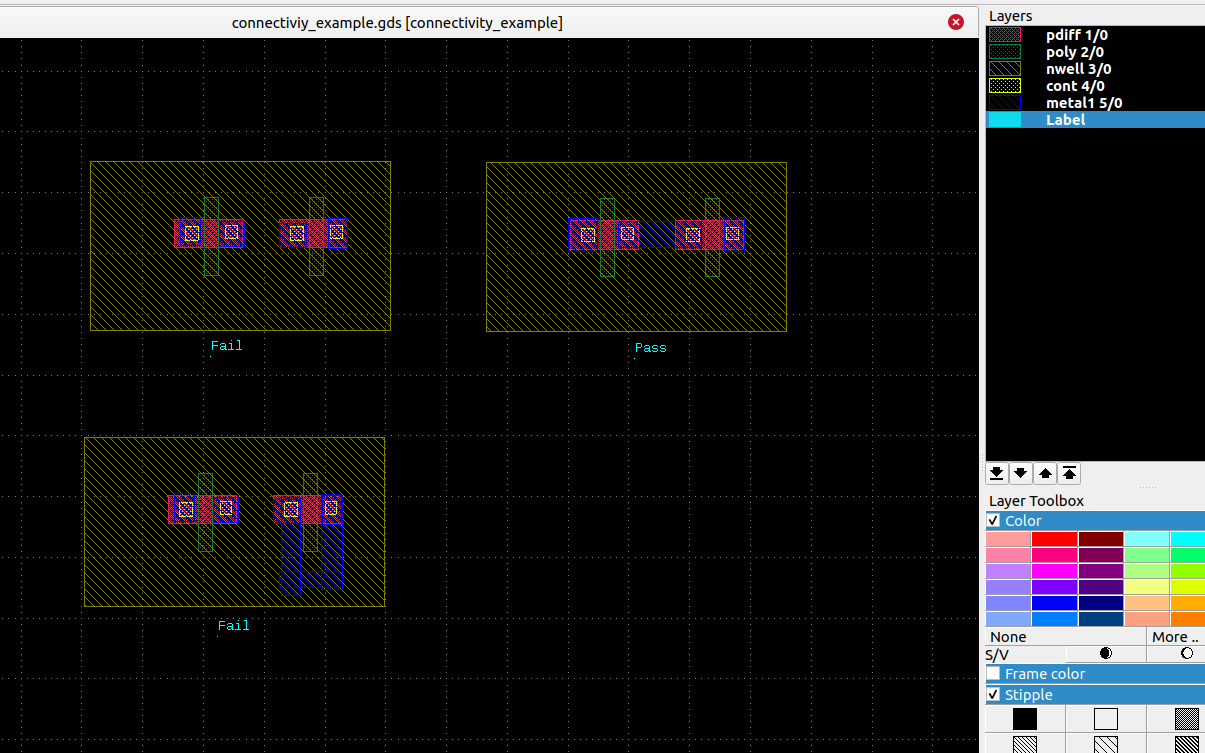
@atork I feel that this is not exactly what we are talking about here. Are you thinking of something more simplistic? I mean, it's possible to code a simple DRC check that covers exactly the cases you sketched in the screen shot above, but what is the generic specification? For example: does the wiring have to be inside the stamp polygon? Will it be only about MOS transistors of the kind you sketched above? May the wiring cross metal layers?
Matthias
Hi @Matthias ,
It could be any stamping not necessarily MOS devices. For example an ntaps, you can't have 2 ntaps on the same NWELL that connected to different nets. Assume now that we don't allow connectivity through NWELL for example.
Regards,
Amro
Also, the metal can be connected anywhere not necessarily above the NWell.
In the example, LVS should produce a layout device with
no schematic match. So the problem would be caught.
Does it matter -how- you catch an error? More than just
time spent getting there (DRC precedes LVS usually)?
I wonder whether what's needed, is a "meta-layout" like
what Brand X produces along the path of layout extraction
and connectivity verification. That is, random polygon layout
is transformed into one with only interconnect purpose layers,
and tiny "instance" symbols for devices, where every
interconnect-layer polygon has now an attached net name
property.
From this kind of database, it seems it would be straightforward
to look at (say) metal enclosing contacts on valid tap layers
for their attached netName property and call out any unequal?
But this all needs the extraction of connectivity. Since you say
that this connectivity can happen -anywhere- I don't see a
polygons-only approach bearing fruit, unless you duplicate
the whole extraction process on the full top level. So, better
to put it to use and take what it gives you?
"You" being anyone with a clue and spare time, which I'm not.