Howdy, Stranger!
It looks like you're new here. If you want to get involved, click one of these buttons!
Quick Links
How to specify W,L of resistor

Hello @Matthias ,
I trying to understand How does Klayout specify W, L of resistor in this case, Can you explain?
r_body = polygons(32, 0)
r_connector = polygons(31,0)
pin = labels(131,0)
connect(r_connector,pin)
extract_devices(resistor("Res",1),{ "R" => r_body,"C" => r_connector })
result:
circuit resistor ();
device Res $1 (A=B,B=A) (R=1.02877697842,L=0.143,W=0.139,A=0.010472,P=0.564);
end;
Thank you,
dai
Comments
Hello @dai,
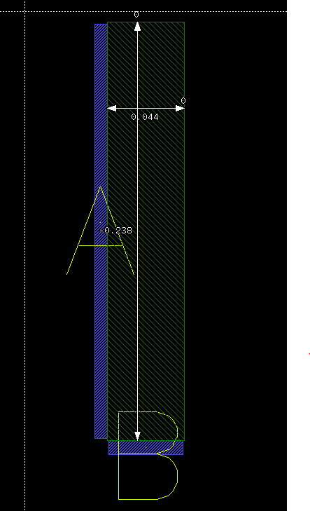
So the blue patched are your terminals? That is kind of strange - usually they are connected on opposite sides.
The computation is L and W assumes a rectangular geometry with two ends being entirely assigned to "contact". The computation follows this scheme:
W is then computed as "total_length(w_edges) / 2" and L is computed as "total_length(l_edges) / 2".
In your case this leads to W being the average of the lengths of the blue stripes and L the average of basically nothing and the long path at the top and right side.
Matthias
Hello @Matthias
Yes, it is terminals.
i trying extract resistor of polygon shape(L,T.. shape), i split polygons to squares and each square is a resistor so it form resistor like that. Here is a example.
Thank you so much.
dai
I see - I guess my approximation is kind of crude for this application, but basically W and L should should give some average path length and width. Approximately.
Matthias
Hi @Matthias
BTW
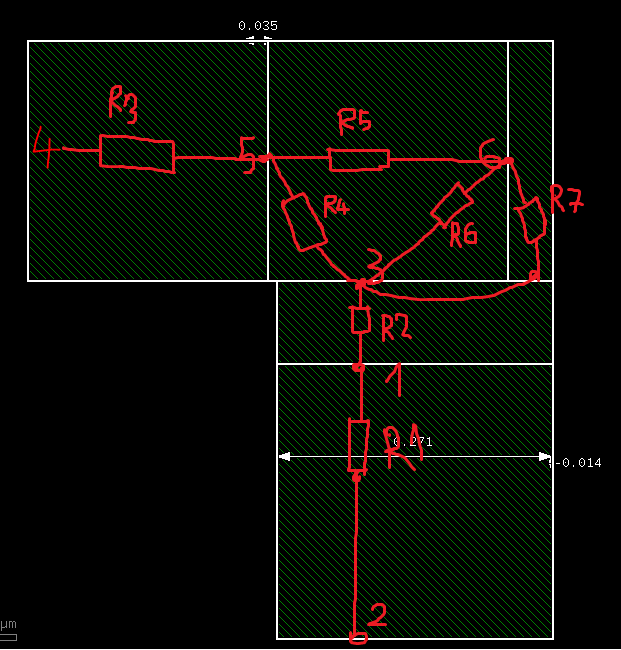
Have any function help to calculate resistance from node 5 to node 6 in this picture?. I can not use netlist.simplify Because it combine all resistor to one. I trying to flag where is high resistor compare others.
Thank you so much!
dai
It looks like an over-elaborate version of the old school
"counting squares and corners" approach. For a fully
ortho resistor, seems like you could collect rectangles
(w/ orientation relative to current-flow axis, for squares
calculation apiece) and corners (treated as half-square)
pretty straightforwardly?
Now the contact cartoon makes zero sense, there's a
trivial gap where resistance will be way low irrespective
of bulk sheet resistance and further-out geometry. It
also does not match the latest "squares" figure, in the
contact-location aspect.
@dick_freebird Looks to me like the approach is to subdivide into pieces with a fixed dimension. So the small portion is a left-over part ...
Matthias
Thank you, @dick_freebird and @Matthias
I think i have to subdivide net into pieces because my net is complex and layout guys just want to show resistance between two specified points that they can select.
dai
Design resistors are (almost) always simple rectangles with terminals located on the opposite sides, corner to corner. Then you get a simple resistance formula: R=W/L*rsh.
For complex (non-1D) layouts like this, you need to mesh your area, apply proper boundary conditions, simulate, integrate the current along your ports / boundary, divide voltage by current, to get the resistance.
You can either spend some time doing that, or use a free field solver, or buy a commercial tool.
It's a tradeoff between your urgency, capabilities, money you are willing to spend on this, and guaranteed speed of getting the results and their quality.