Howdy, Stranger!
It looks like you're new here. If you want to get involved, click one of these buttons!
Quick Links
Problems when extract the MOS4 Transistor with override of GenericDeviceExtractor, pin Well empty.

in Verification
I wanted to implement a custom parameter calculation for Mos Transistor in KLayout LVS, so I used a method that overrides the GenericDeviceExtractor class.** Then I ran into a problem, the "Well" extraction result was empty.**
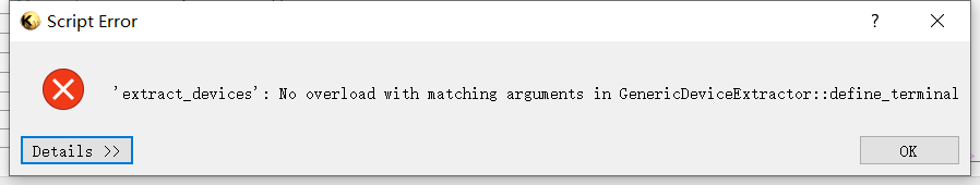
An empty w(well) will cause define_terminal(device, RBA::DeviceClassMOS4Transistor::TERMINAL_B, 4, w[0]);to not work, the error report is as follows:
$dbu_value=dbu
class MOS4Extractor < RBA::GenericDeviceExtractor
def initialize(name)
self.name = name
end
def setup
define_layer("SD", "Source/drain diffusion")
define_layer("G", "Gate input ")
define_layer("W", "Well ")
define_layer("tS", "Source/drain diffusion")
define_layer("tD", "Source/drain diffusion")
define_layer("tG", "Gate input ")
define_layer("tW", "Well (bulk) terminal output ")
register_device_class(RBA::DeviceClassMOS4Transistor::new)
end
def get_connectivity(layout, layers)
conn = RBA::Connectivity::new
conn.connect(layers[0], layers[1]) # collect touching contacts
conn.connect(layers[1], layers[1]) # combine resistor shapes into one area
conn.connect(layers[0], layers[0])
return conn
end
def extract_devices(layer_geometry)
sd = layer_geometry[0]#device
s = sd[0]
d = sd[1]
g = layer_geometry[1]#device
w = layer_geometry[2]#device
puts layer_geometry
s_region = RBA::Region.new(s)
d_region = RBA::Region.new(d)
g_region = RBA::Region.new(g[0])
seed = g_region
perimeter_coincide_s=0
perimeter_coincide_d=0
s_edges = RBA::Edges.new
(s.each_edge).each {
|n|
s_edges = s_edges + n
}
d_edges = RBA::Edges.new
(d.each_edge).each {
|n|
d_edges = d_edges + n
}
seed_edges = RBA::Edges.new
(seed[0].each_edge).each {
|x|
seed_edges = seed_edges + x
}
(d_edges&seed_edges).merged.each do |e|
perimeter_coincide_d += e.length
end
(s_edges&seed_edges).merged.each do |e|
perimeter_coincide_s += e.length
end
w = (perimeter_coincide_s + perimeter_coincide_s)/2*$dbu_value
l = seed.area*$dbu_value*$dbu_value/w
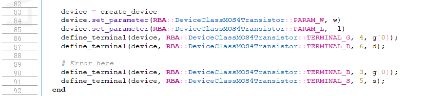
device = create_device
device.set_parameter(RBA::DeviceClassMOS4Transistor::PARAM_W, w)
device.set_parameter(RBA::DeviceClassMOS4Transistor::PARAM_L, l)
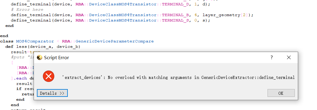
define_terminal(device, RBA::DeviceClassMOS4Transistor::TERMINAL_G, 2, g[0]);
define_terminal(device, RBA::DeviceClassMOS4Transistor::TERMINAL_D, 1, d);
# Error here
define_terminal(device, RBA::DeviceClassMOS4Transistor::TERMINAL_B, 4, w);
define_terminal(device, RBA::DeviceClassMOS4Transistor::TERMINAL_S, 0, s);
end
end
But when using the default extract_device, the w pin is extracted correctly. What is the cause of the empty well (layer_geometry[2]) and how should I deal with it, how to extract the correct w pin?
In order to reproduce this problem, I added the test file in the attachment.
Comments
Basic JI NMOS may have no "Well". Common on older
technologies that had only one (or no) VT implant.
You might elect to make one, to give the generic extractor
"something to chew on". And put it on a layer that you can
stream in / out but doesn't make glass in the end.
@Bian Very simple")
I think that is because you have used the "w" variable for both the width value and the well layer.
Matthias
@Matthias
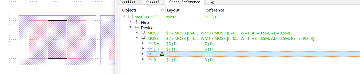
Sorry, it was a stupid mistake, I changed it once, but that's not the essence of the error, layer_geometry[2] is still empty
"define_terminal" expects a single polygon. You supplied a polygon to G (through
g[0]), to S (throughs=sd[0]) and to D (throughd=sd[1]). But not for W which is aRegion(a collection of polygons).Normally, the bulk terminal is something "below" the device - I used the gate polygon for the bulk terminal. The well layer usually is not included in the input layers. Instead, the gate shape is computed as a boolean operation including the well layers. So a PMOS gate is always inside the n well. If you compute PMOS gate shapes and pass those as "G" layer to
extract_devices, the well layer is included implicitly.One additional note: the layers are intentionally split into inputs ("SD", "G") and outputs ("tS", "tD", "tG", "tB"). You take shapes from the inputs, and place terminals on the outputs. That way you can have one
SDinput layer, but two outputs (tSandtD). For example, for the gate layer, you use some computed recognition layer, but you will place the gate terminal on the original poly layer, so it gets connected with the poly routing.The layer ID's used in
define_terminalare zero-based indexes in the orderdefine_layersis called. In your case for example,sshould go totSwhich is layer index 3, not 0.Matthias
@Matthias
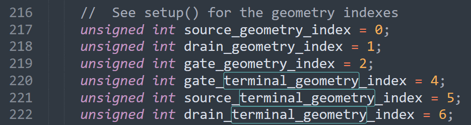
Thanks for your suggestions! You mentioned that the index of
tSis 3. I found this in file dbNetlistDeviceExtractorClasses.cc: ****The index of
tShere is 5, should I follow the settings in the source code about this index, or is there another Doku that I can refer to? I didn't find the corresponding introduction in Dokumentation.Then it is about the extraction of

Well, thans for your reminder, in the last year I asked a question about the extraction of Diode, where you explained to me that the terminal configuration should use polygon, w is the region and w[0] is the corresponding polygon, this I already know due to your advice.https://www.klayout.de/forum/discussion/2178/problems-encountered-when-changing-the-terminal-declaration-in-the-device-class#latest
So I have tried to use
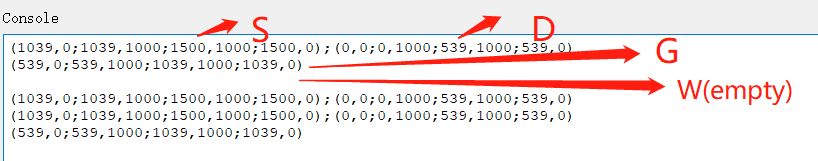
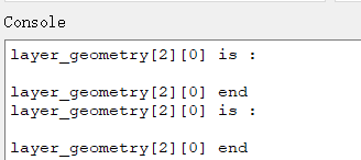
layer_geometry[2][0]as input directly. The result is the same because Well is extracted as empty(layer_geometry[2]is null), which is strange because Well can be extracted when using the default extractor.Output in Console for
layer_geometry[2][0]Default extract_devices, **
**Output
Bwith defaultextract_devices, ****Output
Gwith defaultextract_devices,Output
GundBis different, i want get a same OutputBas this defaultextract_devicesin customextract_devices.But i still don't know how to properly modif
If I use
Gas thedefine_terminalforBThe result of connectivity compare is red
Is this a bug? Maybe
layer_geometry[2][0]should be extracted as nwell's polygon, not null.I don't understand this bit about making G be the B contact.
Active is the B region. S, D and G sit atop parts of it. Maybe
you just want to make PWell = Active andnot NWell and use
that to identify the PWells. Contact to PWell is global Psub
andnot NWell. Contact to global Psub (and PWell) is P+
but often the contact is through Psub to a remote P+ "tap".
Your connect statements need to allow that chain of
ohmicness.
@dick_freebird
That's not the point, the main thing I don't understand is why layer_geometry[2] is null, extracting through the default extract_devices is not null, even though I used the same input. Even without setting the define_terminal part, layer_geometry[2] should not be null, which is not normal, and as you said, it should include G S D
@Matthias
Since
wandtware not used as input inlayer_geometry, how should we setterminal_Bfordefine_terminal, or how do we get list of terminal?In fact about bjt I had a similar confusion, I could extract the device but could not customize it to set the correct TERMINAL_C connectivity
@Matthias @dick_freebird
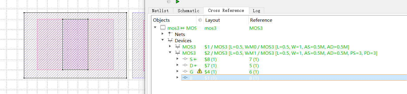
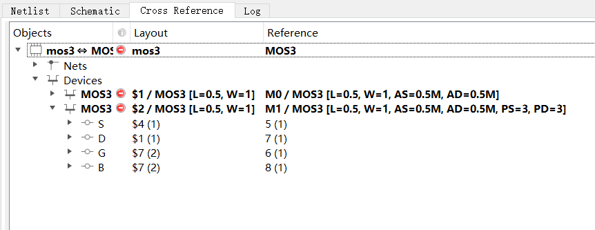
I can get the right result now.
Thanks very much for your Help!!
The correct version that can finally be run:
Do you suppose that you could write a little bit of "wrap-up"
that tells the problems, their cause and their solution apiece?
Clean example is fine, but ability to recognize what the
errors / misbehaviors are trying to tell us, comes from
"learning from mistakes" along the way. Preferably,
"somebody else's".
Getting to a "KLayout LVS Cookbook" is a good goal.
Starting with "For Dummies", would be my speed.
Well, custom device extractors are already "advanced level" ...
There is a worked-out example for a custom extractor here: https://gitlab.com/klayoutmatthias/fsic-2022-demo-files/-/tree/main/klayout-talk/lvs/custom_device
There is also talk of mine where I tried to briefly explain the concepts: https://peertube.f-si.org/videos/watch/bd7d02dd-73d9-4238-862e-6c594a2dc91c
But I think there are some problems in the code above: it is lacking a very important think which is the "connect" statement involving the well layer.
The connect statements inside the device extractor are not making a physical connection but help collecting the clusters of shapes that are need to form the device.
With these layers:
the connects will do:
So you do not pull well shapes. You need to add something like
to pull the well shapes over the gate area.
In your code, you pass poly to the "G" layer. Don't do that!. The get shapes should be localized ("device recognition") shapes, so use something like "diff & poly". Otherwise the device extractor will see long poly wires or similar.
We have "conn.connect(layers[1], layers[1])" above to collect all connected islands in case the gate consists of more than one shape.
And don't use polygons from output layers. Only use them for placing terminals to. So don't use
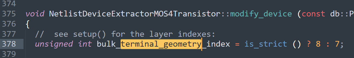
layer_geometry[5][0]because you have designed layers 3 and above as output layers.You have added the "W" layer (for reasons I do not understand), so you cannot simply reuse the layer indexes from the MOS4 extractor's source code. If you want to output terminals, place them on "tW" which in your case is layer 6 and will allow you to specify an output layer for the bulk terminals. Usually bulk does not have an input as there is no geometry defining the "bulk" area (others than just covering the device). You do device differentiation in terms of computing device specific gate regions (e.g.
pgate = nwell & poly & diff) and using that in "extract_devices" for the "G" input. This way you do not have to define different device extractors for NMOS, PMOS etc.Matthias
This (the actual construction and connections between
layers) is what I was getting at. I think that inspecting the
cutaway and level-plot figures which must attend the
layout data for the process, should lead to sensible
layer-logic and connect-logic and without doing, the logic
that results will probably be kooky / buggy / wrong.
And still my gut says the problem is, there -ain't- no
steenkin' PWell without somebody makes with the
Booleans. Layertable would tell. From what I see you
don't have enough input layers to make a CMOS device
set. Declare some later, sure. But not enough real input
to populate them right.
@Matthias

Thanks very much for your advice, it has helped me a lot!
In fact this code is a test case I made to reproduce my problem, so the specific Layer assignments and calculations are virtual, as I am not allowed to publish the rules file of the Technology being used for legal reasons.
Accordingly, I added W because the device defined in the rules file of the Technology used contains the definition of the W layer, For example:
Because different devices use different algorithms to calculate the parameters, for each device I have to construct a separate extract_device, which I have been working on for a long time and will finish recently.
I am a Diplom student at TU Dresden and both my Studienarbeit and Diplomarbeit revolves around using KLayout as an alternative to Cal ibre for LVS.
@dick_freebird
I'd be very happy to do it, but it wasn't until about seven weeks later that I had enough time to do that.
Until then I can write a little bit of "wrap-up" to explain my misbehaviors