Howdy, Stranger!
It looks like you're new here. If you want to get involved, click one of these buttons!
Quick Links
MOM capacitor extraction

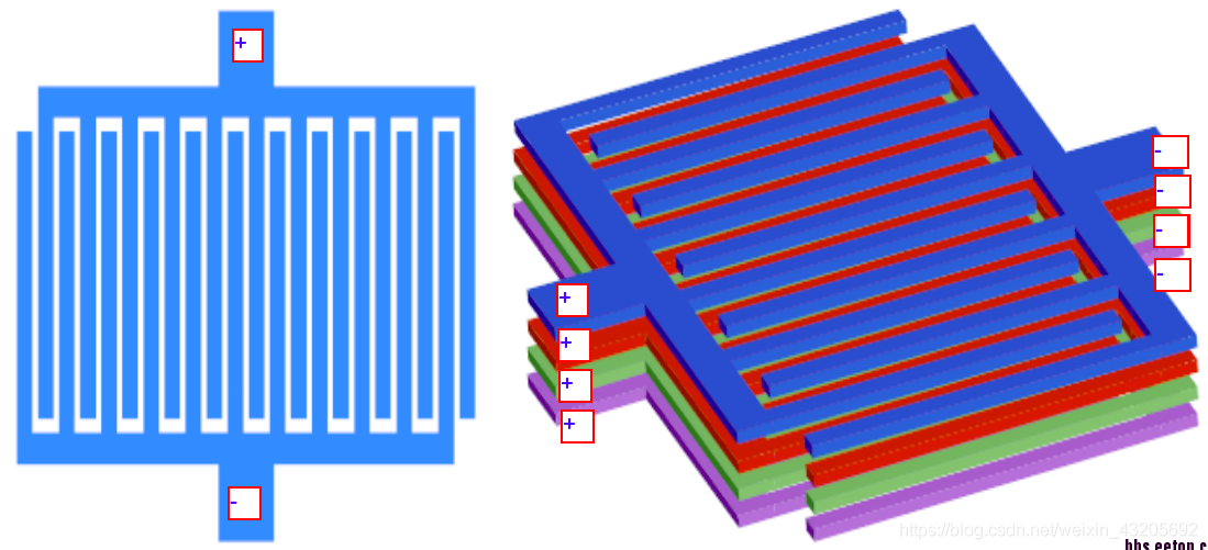
I found in the manual that it can extract vertical capacitors. However, I wonder if it is possible to extract MOM capacitor which constructs capacitor in the same metal layer by using multi-finger structural.
Comments
That's going to be tricker because it's a 3D problem (vertical and lateral fringing dominates). An extractor -could- handle it but whether this one does, I do not know. Would be some more elaborate code than a vertical only, plate-plate capacitance extraction.
I imagine that if two parallel lines extract with a mutual C, the extractor can handle the larger bundle. Might take that test case to the mat and see?
If you find the extractor as-is unworkable, and are willing to make a PCell, a workaround could be to embed recognition features that declare this line-pile as a "device", and the PCell places along with the metal geometries a "param reflection feature" that returns the figured terminal-terminal and bottom-"plates"-substrate capacitances by a geometry value.
As an example, "back in the day" we would not write extraction scripts to get the emitter dimensions (L, W) from N+ polygon data - we would instead make the PCell lay down a "width/drawing" rectangle with X=1, Y=WE and a "length/drawing" box with Y=1, X-LE; extractor had only to find that "width" rectangle and take its area (so orientation does not matter) and there you go. Presuming you did not molest the PCell "guts".
This all goes to PDK architecture and use of adjunct (non-printing) layers to ease the pain of verification script coding.
It may be noble and heroic to extract everything from plain printed layer data. But who's got the spare time for heroics?
Well, open source coders, obviously. But there's never enough heroes when you wanted it yesterday.
@dick_freebird Thanks, this is exactly what I have in mind too (I do not feel heroic enough to extract these things from plain metal polygons).
@William1 You really need a kind of marker layer which allows you to recognize the capacitor. Recognizing a specific comb structure as a capacitor without marker layers is tedious to code and likely to give you false devices in the end.
Here is a proposal how to do that:
The dashed white line is the cap area marker. Note that is covers the comb area, but does not reach into the metal connecting the fingers. This is important for this scheme to work.
The script is written with a loop to keep it compact. I hope the comments explain the idea.
And here is my output:
The idea is that the capacitance scales with the cap area which is roughly true for a given width and space. As this is just the nominal value, I think this assumption is valid. In my case the area of the cap layer was 33µm² which corresponds to 33fF because I used 1fF/µm². Times four (because of the four layers) gives 132fF.
Matthias
On the note of marker layers, you might like to take a dive into
the mainstream foundry PDK (if this is meant to get real) and
look for these kinds of layers ("capacitor/drawing"?) and also
see if there's a multifinger MOM cap already drawn in their cell
libraries - it might hold style-cues and clues about what your
eventual tape-in will be looking for.