Howdy, Stranger!
It looks like you're new here. If you want to get involved, click one of these buttons!
Quick Links
LVS not recognizing interdigitated devices

Hi,
I am working with some transistors that have an interdigitated source and drain under the gate and I have not manage to extract the device with the mos3 function. Is possible to extract this type of devices with their dimensions?
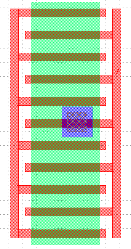
The device shape is as follows:
Thanks in advance,
BarDesigner
Comments
"Shape", OK, but that doesn't look like a fully formed MOSFET.
If green is Active then where's the gate? If green is gate, where
is well(s), active, etc.?
Depending on the extract function's code & settings, you
might expect to see a plurality of single-stripe W/L devices
extracted in a raw netlist. "Brand X" calls on "permuteParallel"
per-device-species-defined enable variables to bridge between
what may come from a simple polygon extract, and what's on
the schematic (i.e. (N) 10/0.18 nmosl match one nmosl with N
fingers of 10/0.18 if you allow parallel devices to permute to a
single),
Where, how or whether this happens in klayout extract or LVS,
I don't know.
However if you get no devices at all I'd be looking to construction
details, and how you're teloling "mos3" what's what to key on.
Thanks for the interest dick_freebird, regarding the device is not a conventional mos device since is made with organic compounds and all the green area is the gate that at the same time is the active.
But this is not the issue since if I made only one channel device and with the appropriated layer operation, the device extractor is working properly, the problem starts whit the interdigitated source and drain.
Can you explain little bit more about the "permuteParallel" call, I can not find information about it in the searcher.
Thanks,
BarDesigner
The "permuteParallel" is one of the topology-massaging
rule options in "Brand X" LVS (they shall not be named).
A netlist "refinement" stage precedes the connectivity
verification, or mops up after (I dunno, a CAD developer
I am not - but I've seen the fill-form in circumstances
where sonebody's "real" developer neglected this and
so the schematic and layout mismatch even though they
don't, electrically).
In the LVS reference you might look at "align" as maybe
doing this (it claims to massage netlists) and "equivalent_pins"
(which in other cases might get you past stuff like calling a
symmetric MOFET's S, D swap an error when it is not, for
the specific device type). But how to use, I got nuthin'.
Thanks for the answer, I have been testing with the insights that you give me, but I can not manage to extract properly the interdigitated device. Lets see if someone else had manage or have some other idea to test.
BR,
BarDesigner
Maybe step back a couple, and show what -does- result. Like,
no "device" at all, or a herd of small ones where you wanted
one representing all fingers?
Maybe modify your rules deck to spit out to "debug layers"
any layer Booleans you think should produce a region for
such-and-such? If using one of the "canned" extractors,
maybe duplicate their code in a macro that insteads does
the logical ops but leaves you with inspectable layer objects
for each "logical input" (I dunno, body, gate, source, drain?).
Who knows, maybe it's just that there's no "body" and the
logic bombs for that.
Not being too clued on klayout, but having seen plenty of other
extract decks and PDKs, I wonder whether the issue might be
that "MOS3" still wants to know what the body is, somehow, so
it knows what's in and what's out. Maybe needs "active area"
(= gate) asserted to whatever the inputs-list is? Or maybe there's
something funny about mos3 when active and gate are identical
(quite abnormal for CMOS silicon). Maybe you want to make an
explicit "active" layer to feed the extractor, it's quite common that
"artificial layers" are created to give extract and LVS rules "bite
sized morsels", they can be finicky eaters.
Hi @BarDesigner and @dick_freebird,
The MOS3 device is suitable only for specific geometries which are resembling a planar MOS transistor:
(https://www.klayout.de/doc-qt5/manual/lvs_device_extractors.html).
So there must be some drain and some source region separated by a gate and the gate must be rectangular (!).
It is quite common to have multiple transistors in parallel for increased width. In that case, multiple transistors are extracted and later combined into big ones. I assume this concept can be applied to your device.
But I need some more detailed explanation where you have gate and source/drain features. Maybe the device isn't even a lateral one?
If the device is difficult to cast into the MOS3 scheme, it is basically possible to implement custom extractors generating MOS3/4 device models. That however is not done with a few lines of code.
Matthias
Thanks both of you for the responses and the ideas in order to fix the issue.
I have taken the inverter example of the testdata from github. I added an extra finger to the layout of the NMOS and the LVS is extracting two devices and not one with double W as expected.
How should be implemented the parallel transistor topology to being extracted properly?
About my devices I do not think to get a similar shape to the classical ones will be a problem, so if I manage to solve the modified example my case can be arranged to.
BR,
BarDesigner
Then the chore of combining them to a single multifinger falls to either an intermediate "netlist optimizer" or this is a feature of LVS itself. But that step wants its own "membership rules" (like the merging of fully parallel devices).
Maybe MOS3 in in that club a priori. But even so all 4 nodes need to be known (one being assumed, the B, and that assumption would need to be led else unique "stuff" might be made up (like a unique "B" apiece, lacking any better idea?).
So how about that - by inspection do the FETs in the netlist have, or have not all four terminals identically assigned, such that an "optimization" could be done but is not, or could not be done "because"?
If there is to be such a cleanup pass it might well have to be invoked explicitly. That would need someone who's read the manuals and howtos....
The LVS deck from the example does not include the device combination step. You can add this by using
before "compare". This is basically the idea that @dick_freebird mentioned in the last post: this is the "netlist optimizer" step. It is intentionally made a separate step so it can be configured - e.g. confined to specific device types.
There are some such optimizer steps of which most are combined into a single utility function:
See more here: https://www.klayout.de/doc-qt5/manual/lvs_tweaks.html#h2-52
Matthias
Thanks for the responses. With the combine_devices is now working like a charm.
BR,
BarDesigner
Cool")
Thanks for that feedback.
Matthias