Howdy, Stranger!
It looks like you're new here. If you want to get involved, click one of these buttons!
Quick Links
Reduce split gate option in LVS

Hi Matthias,
In LVS using some complex Flip Flop cells, I encountered the case that Klayout required MOS device reduction option for the extracted net list as shown below. (Sorry "Attach image" file failed to upload at present.)
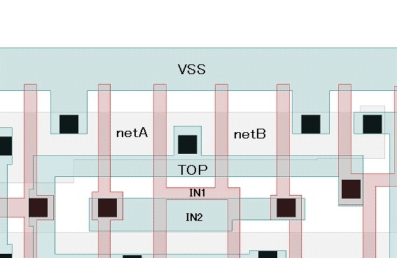
Extracted circuit
M1Up netA IN1 TOP VSS NMOS L=1U W=1U
M1Low netA IN2 VSS VSS NMOS L=1U W=1U
M2Upr netB IN1 TOP VSS NMOS L=1U W=1U
M2Low netB IN2 VSS VSS NMOS L=1U W=1U
*please note netA and netB is not the same net.
After reduction
M1 netC IN1 TOP VSS NMOS L=1U W=2U
M2 netC IN2 VSS VSS NMOS L=1U W=2U
This reduction option is called "LVS REDUCE SPLIT GATE" in Mentor Caliber for example.
Can this option be implemented for Klayout circuit reduction in future?
Best regarts,
haru_f
Comments
Hi haru_f,
Ok, here's the image:
It's easy to implement if there are four transistors involved (that's just a big "if" then). But basically the chain can be more than two pairs and each transistor can be split into more than gates. Will this be important?
The smartness required in the general case is to conclude that the NetA and NetB nodes are equivalent (== carry the same potential) for symmetry reasons. Hence they can be connected virtually.
There is a famous example where detecting symmetry is also important for reducing devices:
I don't know if such a smartness can be implemented.
Thanks,
Matthias
Hi, Matthias,
Certainly, theoretically possible to extend the number of vertical and horizontal stages. However, this configuration seems to be very limited application for reducing the area of Flip-Flop cell.
The number of vertical stages has a limitation on electrical characteristics, and the number of horizontal stages has an area limitation for gate connection.
Therefore, I think it is sufficient to limit the application to 2 stages for vertical and horizontal.
Thanks,
haru_f
Ticket for this was created;
https://github.com/KLayout/klayout/issues/482
Hi, Matthias,
I found this type of "split gate configuration" existed in large size NAND/NOR gate standard cells.
Thus, could you support up to 4 vertical stacks?
Thank you very much in your efforts in advance.
Thanks,
haru_f
Well ... this won't be a simple "if" then ...
Let me check what's possible. I have not started with this issue yet as I'm a bit short of time right now.
Regards,
Matthias
Hi, Matthias,
It's okay.
Until it can be ehhanced, I use extracted netlist as a temporary schematic netlist for those cells.
Thank you for your effort in advance.
Thanks,
haru_f
I'm thinking about this ... but it's going to be slightly tricky. But I love taking challenges")
Matthias
Hi haru_f,
I have prepared a feature which I think will help you. Here is a brief description:
http://www.klayout.org/downloads/master/doc-qt4/manual/lvs_tweaks.html#h2-178
I'm going to release this soon. Maybe you can give it a try. A preliminary build for Windows (unsigned) can be found here: http://www.klayout.org/downloads/master/ (look for 0.26.4 versions)
Matthias
I will observe that the schematic example posted by Matthias
contains an error, in its assertion that the two forms are equivalent.
They are not, unless you add a connection between the left and
right "drain nodes" of the left-hand circuit.
Reduction is good, until it isn't - like, if you go past true equivalence
and create topology that was not originally so.
Hi, Matthias,
Thank you for your effort!
I checked all type of NAND/NOR gates by pre-0.26.4 version.
Following keywords were added in the script.
#Split gate option
join_symmetric_nets("NAND2X")
join_symmetric_nets("NAND3X")
join_symmetric_nets("NAND4X")
join_symmetric_nets("NOR2X")
join_symmetric_nets("NOR3X")
join_symmetric_nets("NOR4X")
Great!
Following gate types can be matched normally.
NAND2X* NMOS 2stage x 2stage
NAND3X* NMOS 3stage x 3stage
NAND4X* NMOS 4stage x (2stage x 2stage)
NOR2X* PMOS 2stage x 2stage
NOR4X* PMOS 4stage x (2 stage x 2stage)
Inaddition, a complex Flip-Flop including NAND2 type split gate can be matched.
join_symmetric_nets("DFF???")
However, only NOR3X* PMOS 3stage x 3stage could not be matched.
Could you please checked the NOR3 type gate ?
Thank you very much in your efforts in advance.
haru_f
Hi haru_f,
Essentially the algorithm should be universal. Is it possible to paste a layout-extracted netlist for a NOR3x3 stage (before join_symmetric_nets) so I can take a look?
I assume that NOR3x is identical to NAND3x if you swap NMOS/PMOS and VDD/VSS, right?
Thanks,
Matthias
Hi haru_f,
This is a test case which works for my version (intentionally messed up a little to test the algorithm):
It reduces nicely to:
Is this basically how your NOR3x testcase looks like?
Matthias
Hi, Matthias,
I'm very sorry. It was my mistake.
I forgot to replace the NR3X* cell netlist from "exracted" to "original".
I could confirmed that this option works perfectly.
Thank you for your effort!
Thanks,
haru_f
Very good")
I'll release the feature then with version 0.26.4.
Kind regards,
Matthias