Layout view of resistors

edited March 2021 in Layout

Hello, I am trying to learn the concepts in LVS and device extraction. I am using an LVS script to automatically generate netlists.
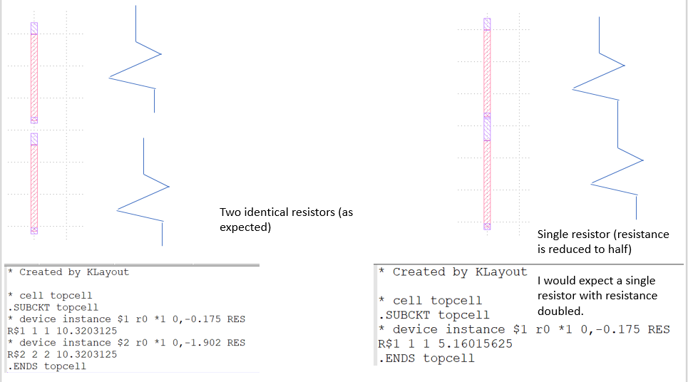
I have a basic question. I don't understand why the resistance reduces to half even though I connect the resistors in series (or at least I think I connect them in series :smiley: . But it looks like they are connected parallel)

The following layouts consist of two resistors. One of them has separate and the other has connected resistors. When I produce the netlist you see the resistance values as 10.32 and 5.16. I don't understand why resistance reduces to half when I connect these two resistors. Shouldn't they become a single resistor with resistance doubled (since they are connected in series. -or am I wrong? Are they actually parallel?)

If you can make an explanation it would be really helpful! (By the way is there a reference (book etc. ) where I can check how basic electronic components in layout view look like? (Instead of the logical view)

Thanks!

PS: This is the LVS code I use to automatically generate netlists

target_netlist("resistor2.cir", write_spice, "Created by KLayout")

deep

# Produce LVS report
report_lvs

res_layer = input(1,0)
contact_layer = input(2,0)

bulk = polygon_layer

sheet_rho = 1
model_name = "RES"
extract_devices(resistor(model_name, sheet_rho), { "R" => res_layer, "C" => contact_layer })

connect(res_layer,contact_layer)
#connect_global(bulk, "SUBSTRATE")
report_netlist("resistor.l2n")
# Netlist normalization
netlist.simplify

Comments

  • Whether they are series or parallel depends on
    whether the endcaps are the same net or different.
    The netlisting appears to think they are the same
    net. But "why?" is probably the question.

    Now there's something funny about the two
    endcaps of both resistor segments, as if perhaps
    the "longer" one is also contacting "something"
    (NWell? Substrate? Or just a non-identical detail
    layout?) as is the norm on implanted resistors
    of single stripe - one contact also grabs the
    isolation region. Then if the isolation is treated
    as a "local global net" (i.e. extraction logic calls
    it an ohmic short) than permute-parallel rules
    (forget what klayout calls this) might give you
    the outcome you're seeing.

  • edited March 2021

    Following and testing results are here code follow's
    The test gds can be found here
    https://github.com/hgroller/test_res

    # Drawing layers
    deep
    
    
    nwell       = input(1, 0)
    diff        = input(2, 0)
    pplus       = input(3, 0)
    nplus       = input(4, 0)
    poly        = input(5, 0)
    thickox     = input(6, 0)
    polyres     = input(7, 0)
    contact     = input(8, 0)
    metal1      = input(9, 0)
    via         = input(10, 0)
    metal2      = input(11, 0)
    
    # Special layer for bulk terminals
    
    bulk        = make_layer
    
    # Computed layers
    
    poly_not_res  = poly - polyres
    poly_in_res   = poly & polyres
    
    diff_in_nwell = diff & nwell
    pdiff       = diff_in_nwell - nplus
    ntie        = diff_in_nwell & nplus
    pgate       = pdiff & poly_not_res
    psd         = pdiff - pgate
    hv_pgate    = pgate & thickox
    lv_pgate    = pgate - hv_pgate
    hv_psd      = psd & thickox
    lv_psd      = psd - thickox
    
    diff_outside_nwell = diff - nwell
    ndiff      = diff_outside_nwell - pplus
    ptie       = diff_outside_nwell & pplus
    ngate      = ndiff & poly_not_res
    nsd        = ndiff - ngate
    hv_ngate   = ngate & thickox
    lv_ngate   = ngate - hv_ngate
    hv_nsd     = nsd & thickox
    lv_nsd     = nsd - thickox
    
    # Resistor device extraction
    
    class CustomResistorExtraction < RBA::GenericDeviceExtractor
    
      def initialize(name, sheet_rho)
        self.name = name
        @sheet_rho = sheet_rho
      end
    
      def setup
    
        define_layer("C", "Conductor")
        define_layer("R", "Resistor")
    
        register_device_class(RBA::DeviceClassResistor::new)
    
      end
    
      def extract_devices(layer_geometry)
    
        # layer_geometry provides the input layers in the order they are 
        # defined with "define_layer"
        # conductor is supposed to be "conductor outside marker"
        # resistor is supposed to be "conductor inside marker"
        conductor = layer_geometry[0]
        resistor  = layer_geometry[1]
    
        # the index of the conductor layer (needed to make the terminals)
        conductor_geometry_index = 0
    
        resistor_merged = resistor.merged
    
        # this will be the edge where the resistor turns into conductor
        marker_edges = conductor.merged.edges & resistor_merged.edges
    
        resistor_merged.each do |r|
    
          # identify the edges where this resistor shape ends
          interface_edges = marker_edges.interacting(RBA::Region::new(r))
    
          # form terminal shapes from these edges
          terminals = interface_edges.extended_out(1)
    
          if terminals.size != 2
            error("Resistor shape does not touch marker border in exactly two places", r)
          else
    
            # A = L*W
            # P = 2*(L+W)
            # -> L = p+sqrt(p*p-A)
            # -> W = p-sqrt(p*p-A)
            # (p=P/4)
    
            p = 0.25 * r.perimeter
            a = r.area
    
            d = Math.sqrt(p * p - a)
            l = p + d
            w = p - d
    
            if w > 1e-3
    
              device = create_device
              device.set_parameter(RBA::DeviceClassResistor::PARAM_R, @sheet_rho * l / w);
              define_terminal(device, RBA::DeviceClassResistor::TERMINAL_A, conductor_geometry_index, terminals[0]);
              define_terminal(device, RBA::DeviceClassResistor::TERMINAL_B, conductor_geometry_index, terminals[1]);
    
            end
    
          end
    
        end
    
      end
    
      def get_connectivity(layout, layers)
    
        # the layer definition is marker, conductor, resistor  
        # * resistor is used for extraction
        # * conductor is used for producing the terminals
        conductor = layers[0]
        resistor  = layers[1]
        conn = RBA::Connectivity::new
        conn.connect(resistor, resistor)
        conn.connect(conductor, resistor)
    
        return conn
    
      end
    
    end
    
    # Resistor Definition
    # Assumes a sheet rho of 150 Ohm/Square
    #Define this as you like
    res_ex = CustomResistorExtraction::new("RES", 1.0)
    extract_devices(res_ex, { "C" => poly_not_res, "R" => poly_in_res })
    
    # Define connectivity for netlist extraction
    
    # Inter-layer
    connect(contact,        ntie)
    connect(contact,        ptie)
    connect(nwell,          ntie)
    connect(psd,            contact)
    connect(nsd,            contact)
    connect(poly_not_res,   contact)
    connect(contact,        metal1)
    connect(metal1,         via)
    connect(via,            metal2)
    
    # Global connections
    connect_global(ptie, "BULK")
    connect_global(bulk, "BULK")
    
    # Actually performs the extraction
    
    netlist = l2n_data.netlist
    
    # Write the netlist 
    
    writer = RBA::NetlistSpiceWriter::new
    
    # Netlist simplification 
    # NOTE: use make_top_level_pins before combine_devices as the pin
    # stops the three resistors to be combined into one
    netlist.make_top_level_pins
    netlist.combine_devices
    netlist.purge
    netlist.purge_nets
    
    path = RBA::CellView::active.filename.sub(/\.[^\.]*$/, "_simplified.cir")
    netlist.write(path, writer, "Netlist after simplification")
    puts "Netlist written to #{path}"
    
    
  • Ege_Bey,

    You can find more info located here, Matthias has provided a dummy pdk.

    https://github.com/klayoutmatthias/si4all.git

    Tracy

  • edited March 2021

    Hello! Sorry for my late reply! Thank you very much for your help and providing this nice resistor layout and the code :smile: !

  • Ege_Bey,

    Any time this was buried in the forum and many thanks to Matthias for providing the dummy pdk

  • @tagger5896

    Thanks for the sample. To be frank it seems to be working, although it produces each resistor in a separate cell because that's how it was designed.

    If you want to get rid of the RES2 device cell, use this:

    netlist = l2n_data.netlist
    # removes the RES2 device cell
    netlist.flatten_circuit("RES2")
    

    I have also added this

    report_netlist
    

    At the beginning which gives me this nice netlist view:

    In this case, resistors don't get combined as the middle node is a pin.

    When I remove the "OUT" labels, this pin is gone and I get a nice combination of the resistory in series:

    So my conclusion is that it's working.

    In your previous case, I think the problem was that you shortened the resistors by connecting the resistor layer (which is essentially the body) and the contacts. This makes the body a conductive layer which shorts everything:

    connect(res_layer,contact_layer)
    

    This is also the reason why "R$1" in your right netlist is connected to net "1" with both terminals.

    Classic joke (KiCad version):

    Matthias

  • @Matthias,

    Thanks for the valuable input,
    I am still learning Klayout in's and outs .
    Tracy

Sign In or Register to comment.