Howdy, Stranger!
It looks like you're new here. If you want to get involved, click one of these buttons!
Quick Links
NPN transistor extraction issue

Hi,
I'm writing a LVS script to check my layout and I want to see if someone can help with this issue.
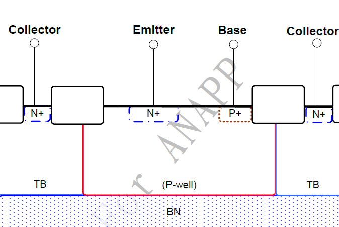
I try to extract a vertical NPN transistor in the layout. The following is the structure of the NPN transistor
I'm using the following script to extract the NPN transistor
emitter = active_outside_nwell & nplus
base = active_outside_nwell & bury_n
collector = bury_n
collector_contact = bury_n & nwell
base_contact = base & pplus
npn_model_name = "NPN"
extract_devices(bjt3(npn_model_name), { "C" => collector, "B" => base, "E" => emitter,
"tC" => collector_contact, "tB" => base_contact, "tE" => emitter})
NPN connect ======================
connect(emitter, contact)
connect(collector_contact, contact)
connect(base_contact, contact)
metal connection
connect(contact, metal1)
connect(metal1, via1)
connect(via1, metal2)
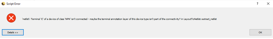
But I can't extract the transistor and it always show me the error message as follows:
Please give me some advise to handle the above issue! Thanks!
Comments
Please format your code using Markdown: a line with three backticks before and after the code will format it
Matthias
Your collector contact should be the stack of contact, Nplus, Nwell, buriedN. You do not have the N+ and contact in your logic. It's possible that contact to NWell could be a Schottky contact depending on surface doping unless you impose N+. Also (can't see) the connect chain from metal to the "contacts" should include the contact layer as a stepping-stone, how else can metal connect to the "contact regions" as-defined?
Thank you very much for all your support.")
Hi Matthias,
I can't see the format look like. I use ~~~ before and after the code. Please help to take a look. Many thanks!
Here is my code for NPN extraction
Hi dick_freebird,
Thanks for your information. I have tried different connection methods. But it is fail to extract the NPN device also. Could you please take a look of the above coding and give me more advises. Thanks!
Terry
@eeterry11 I think you should think simple. Without a sample, it's quite difficult to debug, but I'd propose to change the collector connection to simply:
This should eventually give you the terminals. You have correctly identified non-overlapping regions fro collector_contact and base_contact, so these three connects should give your the three terminals separately.
But as mentioned, an example layout will be helpful.
Matthias
@Matthias the following link can download the layout gds file. Please help to take a look! Thank you very much!
https://www.dropbox.com/s/9dputxuhrlwbdm6/P200241_sample_layout_test.gds?dl=0
Terry
Can you somehow display each of those logical
layers that you are outputting, and see whether
any of them are not giving you what you think?
Maybe one is "malformed" and breaking the
device extraction?
Another thought - I see the extraction of
connectivity, but isn't there some need to
"recognize" the device as such? I don't see
logic for that (what makes the NPN an
NPN, to the extraction?).
In more elaborate kits and tools I'm used
to seeing both type-extraction and
connectivity-extraction to that type's
terminals. Of course I could easily be
confused.
@dick_freebird I did output the logical layers and it is exactly what I want! The following code output the logical layer
But now, I don't know how to create a contact to the collector , base and emitter which the extractor can recognize the device! Thanks!
Terry
Hi @eeterry11,
I'm afraid there seems to be a bug related to collector region. Looks like my test base is too weak on this spot.
I need to debug the problem.
But there is a workaround. I think it's not required to include the collector into the device recognition as base and emitter should be specific enough.
"collector" is optional, so you can replace it by an empty "polygon_layer". This does not give you that errors.
However, the "collector" terminal then will not be the collector region but the base region only. You can make the connection to "collector_contact" via the original collector region though:
I have created an issue for this with an artificial test case: https://github.com/KLayout/klayout/issues/921
Matthias
Hi @Matthias,
I have tried to replace the collector to an "empty" polygon_layer, but the error is here. The following is my updated code. Could you please help to take a look. Do I misunderstanding your meaning? Thank your very much !!
It still bothers me that there is no logic to recognize the device itself. The terminals, OK. But terminals of what? I see where you assign the model name "arbitrarily".
Maybe it's just that I'm used to working in bipolar technologies where there were PCells for a variety of emitter, base, collector combinations - from simple single (1B 1E 1C) through permutations of dual base, dual emitter, ring collector, etc. - 6 each of NPN and PNP in one flow I used a lot. Distinguishing the geometries to point the extraction at the appropriate model, was the first step of the logic, to derive that modelName.
Perhaps in this case there's only one style and only one model so no thinking is required. But maybe that logic would have yielded a finite collector region, or the terms for creating it logically?
@eeterry11 I tried the code of yours with the sample layout and it works for my 0.27.3 version - until it cannot read the netlist. But no error
BTW: I have fixed the issue and the extraction script you proposed initially should work in 0.27.5. Sorry for the confusion.
@dick_freebird Well, there is some logic, but it's built-in.
It's basically possible to code a device extractor, but that's slightly tedious, so some standard device extractors are provided. The "bjt3" device extractor works this way:
Bottom line is: the device recognition happens through the base region mainly. So if you want to differentiate different device types, you first have to select the specific base regions - by means of texts, marker layers, geometry filters or similar. With these base layers - one per device - you go into different extract_devices statements with different classes for the different device types.
I hope this makes some sense.
Best regards,
Matthias
@ Matthias Thank you very much! It doesn't work if there are others devices. I added a marker layer. I can extract the NPN device successfully!
I see. Thank you for this feedback.
This basically means you have other places which are incorrectly recognized as NPN bases (with fake "emitters"). I hope the previous explanation helped with that - a marker layer is definitely helpful as a disambiguator.
Kind regards,
Matthias
I personally favor an all-markers approach where every
device that's placed intentionally, incorporates a unique
marker in its PCell which the extract deck uses to make
the "recognition call" (backed up by a "recognizer" for
device structures containing no such marker, to flag
as error / risk).
eeterry11, I'd like to see your example of marker layer
use, that worked, as it's where my plans headed.