Howdy, Stranger!
It looks like you're new here. If you want to get involved, click one of these buttons!
Quick Links
Extraction MOSFET device in deep mode issue

Hi Matthias,
I have a problem with extraction device in "deep" mode. I also send gds and script to here also, please find attached files.
in my cell is three levels( SUBL1(instance 2 SUBL2)->SUBL2(instance 2 SUBL3) -> SUBL3(1 MOS device )
when i run extraction some MOS devices jump from SUBL3 to SUBL1, i expected SUBL2 include two subcircuits(SUBL3) only, and SUBL3 is one MOS device only but result is unexpected (please see netlist printed below).
my target is after extraction i will flatten SUBL3 and compare with reference netlist but in this case some device instances will be missed in SUBL2(because SUBL3 is empty).
circuit SUBL1 ();
device PCH_SVT_MAC $1 (S=$I4,G=$I6,D=$I1,B=$I2) (L=0.026,W=0.013,AS=0.000897,AD=0.000741,PS=0.164,PD=0.127);
device PCH_SVT_MAC $2 (S=$I1,G=$I5,D=$I3,B=$I2) (L=0.026,W=0.013,AS=0.000741,AD=0.000897,PS=0.127,PD=0.164);
subcircuit SUBL2 $1 ($1=$I1,$2=$I4,$3=$I6,$4=$I2);
subcircuit SUBL2 $2 ($1=$I1,$2=$I3,$3=$I5,$4=$I2);
end;
circuit SUBL2 ($1=$1,$2=$I6,$3=$I2,$4=$I1);
device PCH_SVT_MAC $1 (S=$I5,G=$I3,D=$I7,B=$I1) (L=0.026,W=0.013,AS=0.000741,AD=0.000897,PS=0.14,PD=0.164);
subcircuit SUBL3 $1 ($1=$I1,$2=$I2,$3=$1,$4=$I6);
subcircuit SUBL3 $2 ($1=$I1,$2=$I3,$3=$I5,$4=$I7);
end;
circuit SUBL3 ($1=$1,$2=$2,$3=$3,$4=$4);
end;
If it is a bug or there is any way to resolved?.
thanks you!
dai
Comments
Hello @dai,
Thanks for this nicely prepared test case!
This is a know problem or feature if you like. The devices are correctly recognized, but the appear on a level higher up in the hierarchy than expected.
The reason is the following: A MOS device consists of a gate part and source/drain regions which attach to the gate. The device appears on that lowest level in the hierarchy on which the parts are "complete" (i.e. all connected parts are known). In your case, the source/drain parts of the overlapping transistors are only "complete" on SUBL1 cell level. That is why the respective devices appear only there.
There are a variety of reasons why there is no simple solution to this problem. You case is pretty common in dense SRAM designs, so I have been looking for a solution for this case.
As a now there is the "cheat" workaround which basically says "don't care about what happens further up in the hierarchy" or better: "I promise that I do not plan to modify the device by attaching something from outside the cell". The concept is described here: https://www.klayout.de/doc-qt5/about/drc_ref_global.html#k_17
In your case you can apply it this way:
This will render a netlist where the devices only sit inside "SUBL3" because this cell is treated as if isolated.
I'm aware that this is somewhat ugly, but so far I have not found a better solution for this problem without introducing other flaws instead.
Regards,
Matthias
thanks Matthias,

You guys is so smart, i used calibre tool it have same issue and they have same solution also. it is difficult actually.
Your way work for me, extraction is ok now. But i'm facing pin issue now. when i run lvs for subcell it is correct but when i check top cell with the subcell included, Klayout(0.27.7) extracted two more pins(7 pins) compare number of pin in the subcell(5 pins only) actually. this seem to make the subcell is not match with sub circuit in reference netlist i have. pin added more is two internal nets in the subcell.
I tried to remove two the pins before comparing but i got app crash at compare step.
Have any way to remove two the pins?
thanks you!
dai
@dai Very good")
About the match issue - It's quite difficult to tell from that data what is wrong ... I guess that for some reason also the WL, BTL and BTLB connections are gone. But I really can't say much more here without more data.
Hi Matthias
i'm so sorry take your much time.
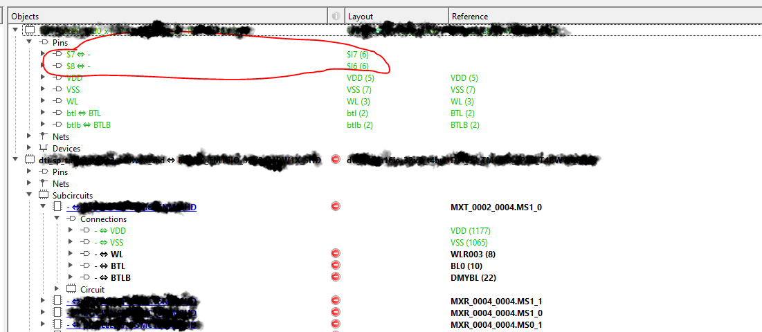
i still try to how does Klayout work with LVS check, i used commercial tool to LVS before run it with Klayout so i'm sure gds and reference netlist matched. Actually, i'm facing with SRAM check, the issue showed when i include bit array to my GDS. I thinks if SRAM has many familiar topologies so may be reason make to flag is not correctly. Example below BL0001(layout pin) should matched BL0001(ref netlist pin)
BL0003(layout) should matched BL0003(ref netlist) But the tool matched BL0001 vs BLB0001, BL0003 vs BLB0003( i checked with calibre layout matched ref netlist). Because this report show Top cell is not correct and in device part show some MOS device is not matched.
I wish i can send test case to you!!!
About two pins added more above, if have any way to avoid it now?. I see we have a blank_circuit function(in help), i tried but it not work for me, it ignore compare for the subcell(made blank) and ignore checking for Topcell too. there any example or guideline more for it?.
thanks
dai
I'm sorry Matthias,
please ignore previous my comment. pin should be fixed on layout. because commercial tool still show correct for this case so i think pin match but i checked manually it should be changed.
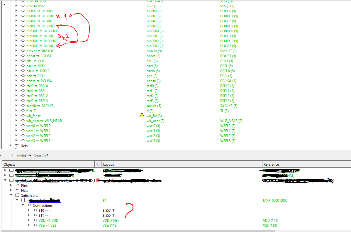
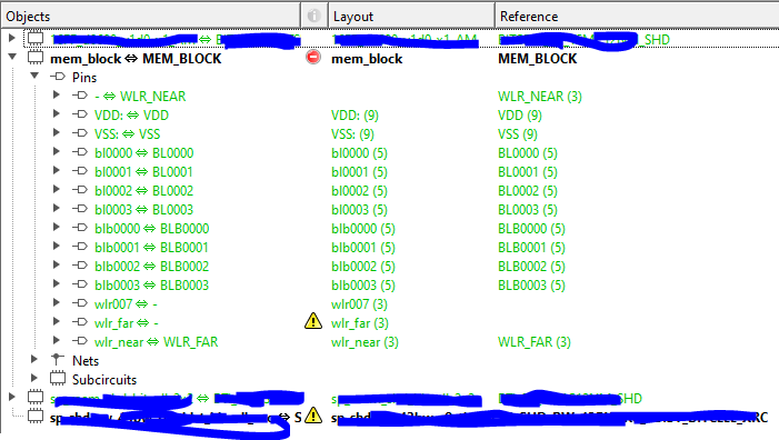
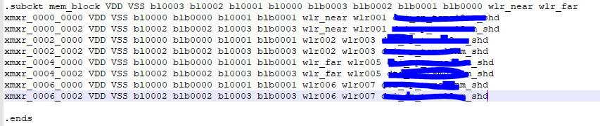
i changed the pins and get result like below. with this result subcell(mem_block) still not passed(because there some pin still not matched).
i see color marked green here, as i know green color just for matched case if i have any confuse here?.
because wlr_far equivalent with wlr_near so i tried to use "equivalent_pins("mem_block", "wlr_near","wlr_far")" but it has no effect.
how can i passed this step to run LVS for top cell?
thank you very much!
dai
thanks Matthias
equivalent_pins work for me now.
dai
@dai Very good ... so what was the problem with equivalent_pins?
Thanks,
Matthias
Hi @Matthias
First time i used name of pins for equivalent_pins function, i think i made something wrong so it not work, after that i changed to used index of pin(equivalent_pins (cirname,1,2....)), it work. now i can run lvs for Standard cell, IO cell, MEM block .
I don't know if have any way to speed up LVS check, now i used "deep" mode also. For big cell i take much time and it can not finish if i run in flatten mode. Here is time i run for one my cell(8MB):
it took around 9 minutes.
thanks @Matthias ,
dai
hi @Matthias ,
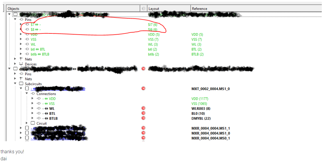
The issue with pin as i showed above
after i remove the un-expected pin to avoid app crash(at "compare" function) i have to find these nets on top of the sub(removed pin)to delete also:
net.subcircuit_pin_count == 1 && net.terminal_count == 0thanks,
dai
Is this effect the same with what's called "seed promotion" in Calibre?
I have not dealt with it myself, but I know from my colleagues that this is a very nasty problem, that does not have a nice solution...
I guess, but I don't have experience with Calibre LVS myself. In general, identifying the true location of a device in the hierarchy isn't always easy. Specifically SRAMs are often build in way hierarchically interwoven way, which makes it very hard to separate the cells from each other.
"cheat" is a way to shortcut some elaborate evaluations which complicate the detection. The price you pay is a loss of precision: for example the source/drain areas may not be correct because they do not include parts which may attach from outside the cell.
Matthias