Howdy, Stranger!
It looks like you're new here. If you want to get involved, click one of these buttons!
Quick Links
How to extract transistor in parallel topology in LVS?

Here is my layout.
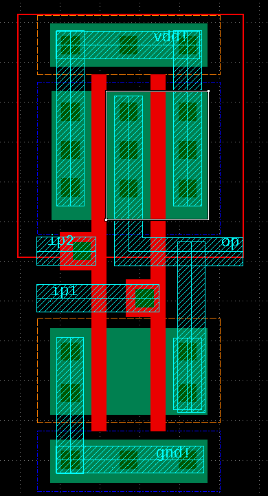
The mos1 and mos2 are in parallel topology. Both of the source of these two mos supposed to connect to vdd. But the source of mos2 is connected to the op in the netlist.
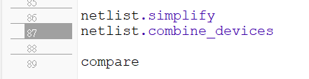
I have added "combine_device" before "compare", but it still can't work properly.
How could I solve this problem?
Thanks advanced!
WENSHIH
Comments
What is missing, is a compare rule that says S, D are swappable
in searching for topology-match. I know I've seen this discussed
but can't remember more.
Or you could go change the schematic so it matches what's naturally
found, but is there "slop" in the process that calls S, D that makes
this stochastic?
I would call the center stripe D and the layout correct, the assignment
seems wrong and you can either fix recognition (e.g. explicit pin
tagging) or comparison (pin permute rules).
Such rules should not be applied willy-nillly, asymmetric devices must
prevent misapplication "escapes".
@dick_freebird
I've seen that discussion either. Is this the discussion that you have mentioned?
https://www.klayout.de/forum/discussion/comment/9014#Comment_9014
I've used the way in this discussion, but I still fail.
That's one such.
"Still fail" is not very informative. Same fail, new fail, ??? The "optimize"
probably needs some specific form and direction....
After I add "combine_device" in my scripts, there is the same consequence as before I add "combine_device", the source of mos2 is still connected to op instead of vdd. Could you explain more about how you call the center stripe D? Also, my language is Ruby.
Sorry about my informative question. I'm still a beginner. If there is anything I could improve, please tell me.
Thanks!
I don't think the devices want or can be combined because they
are not fully parallel. What this situation lacks is enablement of
specific pin swapping (S=D).
Now "combining" could be done -to- the netlist or by bookkeeping
during the compare-grind. But pin-permute has to be a compare
rule because you don't know (or want to keep track of) per-device
detail connectivity, that's what you are trying to verify. But they
should be found in about the same place.
@WENSHIH: source and drain are interchangeable in the standard MOS device. So that is not the problem here. KLayout will basically assign S and D randomly and try both ways during compare (and also during device combination).
"combine_devices" will not have an effect as there are no parallel devices as @dick_freebird pointed out.
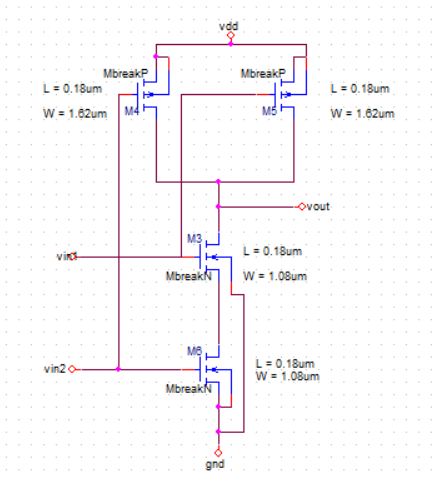
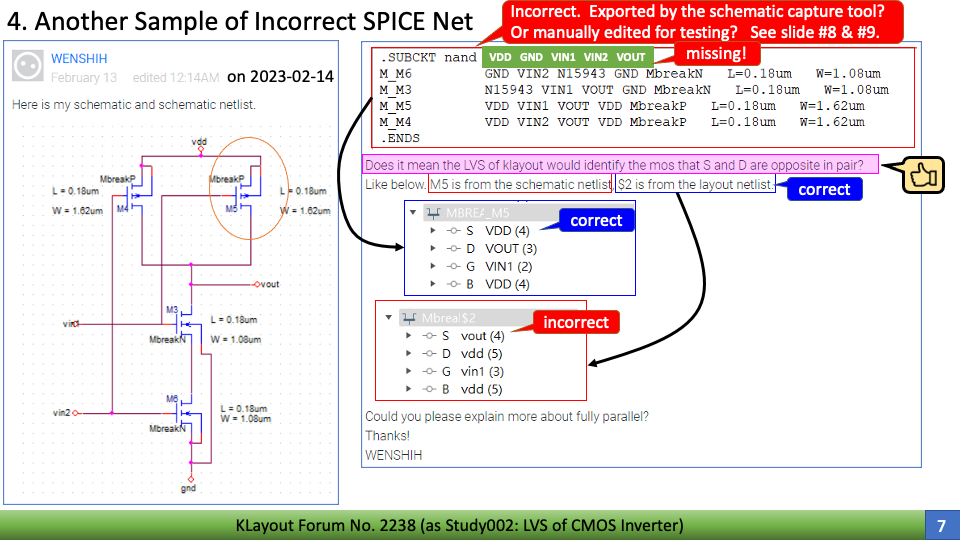
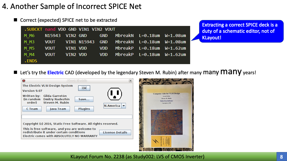
Could you show us your schematic netlist? After all, this is a simple NAND, so that should actually be very simple.
Matthias
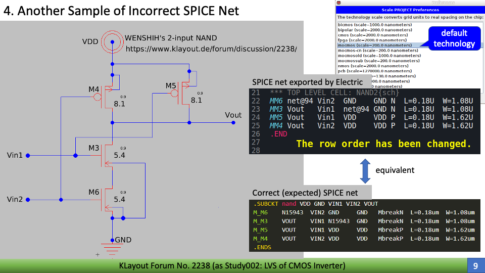
Here is my schematic and schematic netlist.
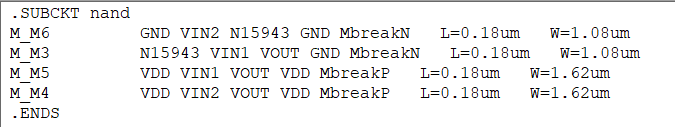
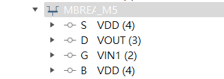
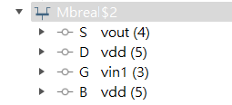
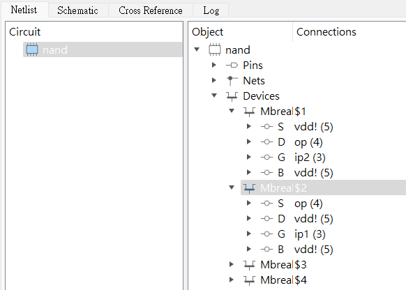
Does it mean the LVS of klayout would identify the mos that S and D are opposite in pair?
Like below. M5 is from the schematic netlist, $2 is from the layout netlist.
Could you please explain more about fully parallel?
Thanks!
WENSHIH
This concerns me. I've been bitten by this when using asymmetric
MOS devices (e.g. drain-extended, no LDD on source). This
behavior (IMO) should be configurable, or an asymmetric MOS
extractor needed.
And then -if- it is configurable, comes the question of whether
it has been configured appropriately.
The outcome suggests that the pin permute is not happening.
But it does appear that every one of your MOSFET symbols
has been placed, or is netlisting, upside down ("D" has S
connections and vice versa).
If your schematic tool will show you the symbol's assigned pin
(like, Brand X will let you select and property-edit on a
schematic's symbol's pin; others display on hover) then it
would be useful to know whether (say) the pin is "D" but is
assigned the connection of "S" terminal, through some
symbol netlisting mess-up, or "D" is reall "D" and every symbol
is really placed vert-flipped.
The way it's netlisted, every FET has to be tested-as-swapped
just for the schematic as drawn to match its netlist. That is not
helping, although maybe the LVS "should" deal with it.
My recommendation at this point is to vert-flip all of the FETs
so that "D is D" and see if that sorts the problem. If it does
then there is something preventing the pin-permute from
working as it should.
But I'm then curious about why (and how not to get hit by it).
Down deep in the Brand X LVS "stuff" you can find a table
which has each known device and a set of pins that are
allowed to swap, for that device. I'm not aware enough about
klayout LVS to know how that all gets managed. But it occurs
to me that OP may have "received the package" without being
involved in any of that, and somebody could have "helped him
to death" and prevented pin permute "because reasons". If
this is indeed modal and settable.
@dick_freebird I'm aware of this")
There is another model, called "DMOS3" (no bulk pin) and "DMOS4" (bulk pin) which treats source and drain separately (see https://www.klayout.de/doc-qt5/manual/lvs_device_extractors.html#h2-192). The price to pay is that you need separate recognition layers for source and drain.
The way I implement swapping is that for "MOS3" and "MOS4" I treat the schematic netlist as given (even if drain is on VDD or GND) and try both ways of the extracted device until a match is found. For "DMOS3" and "DMOS4" the latter step is skipped.
@WENSHIH Just sharing screenshots does not make sense. This is a simple case and no device combination is needed - that only applies to fingered devices which are in parallel (B, S, G and D share the same net). I don't see how the mismatch happens (LVS report), but I also don't see the script, I can't check the layers and derviations and I cannot measure the device dimensions as I do not have the layouts. I can't really help in that case.
Matthias
Given this, I would again suggest that the MOS schematic
elements be flipped so that D (symbol) is D (SPICE) and
see what results. If the compare "gets right" then the D-S
swapping must be somehow compromised. If it makes no
difference then some other problem must be bugging.
You might also just edit the schematic netlist by hand
to swap the D, S terminals "upright".
A question still nags at me, which is whether the native
pin swapping behavior "can be" suppressed; and then if
there's a way, -was- it? All I know is that in some systems,
it's a user-configurable action with pdk-developer-set
defaults.
We have not seen the layout SPICE netlist. The "panel"
showing connectivity truncates the device names and
half of them are collapsed showing no detail. But in
what's shown, appears to be a D-for-S swap on one of
the two displayed FETs, from layout-matching. It would not
hurt for you to try an old school, finger-and-eyeball compare
of the two SPICE netlists, device by device, and catalogue
what doesn't make sense. That might lead to a real clue.
Presuming that the layout side does proceed through a
SPICE netlisting, and not the other way around (schematic
SPICE turned into internal netlist format, and compare
those).
@dick_freebird About the S/D symmetry: the MOS3/MOS4 extractors are by design symmetric. As S/D are represented by the same layer, they cannot differentiate. So if the schematic is correct, there is no switch by which I can tell the extractors (hence the extracted netlist) to use a specific source/drain orientation. So no configuration option.
But the solution is simply to use DMOS3/DMOS4 for asymmetric devices (I think that can be clearly differentiated by the device type). If you do so, there are two separate layers for S and D, and there is no ambiguity.
Matthias
That's good to know.
I'm trying to understand why what should work, does not.
Because there's a lot of use for symmetric MOS. Provided
it's verifiable. Need to know why this is failing, so as not to.
The schematic netlist is correct. All the pins are assigned to the right place and the LVS report that there is no problem. The points which confused me are why does the LVS extract the S and D of layout in opposite and why does the LVS still pass with the correct schematic netlist. In addition, I use the mos4 in my scripts, I know this device is swappable like you said and I guess it's the reason why the LVS pass even the S and D of layout is opposite to the S and D of schematic. But why didn't LVS swap the S and D of layout to the corresponding S and D of schematic?
Thanks for your suggestion and helps! If there is any information I can supply, please tell me.
Here is the test file.
I disagree that "the schematic netlist is correct". I would go
along as far as "it works". But if you inspect the symbols'
wiring and the netlist, there is the fact that (for example)
M_m6 drain and source are swapped in the netlist line
relative to their plain / obvious connection in the drawing,
as is M_m7. And M_m4, M_m5 similarly. At least if you
expect the usual symbol style / locations of pins on it.
Either every device is placed upside-down (which would
have to be some consistent deliberateness?) or the
netlist order is wrong per classic form. This is why I am
keen to understand the flow from schematic to netlist file,
with waypoints at symbol terminal placement and properties
(somebody "could" have made the symbol with "S" at bottom
and "D" at top of PMOS, we don't know until we look, but I
have on occasion made bad symbols and had to chase & fix)
and the netlist template (which also stands capable to
mis-order terminals).
The question of why pin-swapping fails remains, but is not the
only question. We may not know the right question. But trying
to answer the questions we do know, sometimes leads
somewhere.
I've just begun to study LVS, mainly using the Inverter tutorial included in the manuals, and am facing difficulties understanding the results.
Meanwhile, seeing discussions in this post, I was able to make some progress.
In my study process, I am making a PPT as a record of my study.
The 3 slides below are part of it, which will be relevant.
My study keeps going
Kazzz-S
@sekigawa Thanks for these elaborate slides!
I should comment about the "correctness" here: my viewpoint is that "S" and "D" for a symmetric device should both be read as "S or D" as there is no differentiation.
Sure the schematic is not correct if you tie D to vdd, but S and D are only logical concepts for symmetric devices. You could say that for a PMOS, D is the terminal with the lower and S is the terminal with the higher potential. For NMOS it is the other way round.
I guess that for simulation, the models do not necessarily reflect that symmetry, so for that practical reason it is probably better to assign D and S correctly in the schematic. At least if you want to use this netlist for simulation. For the topology however, the assignment is not binding for symmetric devices.
Lacking any differentiating marker, the layout extractor on the other hand will arbitrarily assign S and D for symmetric devices (like said, both terminals should be regarded "S or D"). It does not take any efforts correcting this "mistake". Instead, the netlist compare step regards "S" and "D" as interchangeable, hence the netlists match and all cases.
For DMOS3/4 class devices, the extractor can tell apart S and D and the netlist comparer will no longer regard S and D as interchangeable.
Matthias
Yes, they should be but evidently are not, and I am wanting
to get to the bottom of "why?".
I figure maybe removing known "not-right" from input netlists
might help expose the unknown.
Which thus far, remains unknown.
Let me ask another question which I have not seen specifically
asked: "Which of the MOS extractors are in fact being used?".
It appears to me that this layout is done on a "found PDK"
and perhaps somebody set it up with non-swapping extractors
by default? If you poke into the devices do you find evidence
that D, S are being force-assigned (the recognition layers
mentioned)?
Corrolary activity: If MOS3 / MOS4 -are- being used, how
about switching to DMOS3/4 and making the S/D symbol
connections "correct"? Does that fix anything? Then if so,
why?
I think that showing the extract deck and the layer objects of
the NMOS and PMOS elements might offer clues. If there
is any sort of report file generated during layout extraction,
maybe that too?
@Matthias Thank you for your explanations, which somewhat cleared the fog around me.
@dick_freebird I think your above comments and suggestions are valuable.
@WENSHIH Thanks for your test case, which helped me do my experiments.
Seeing discussions among you, I decided to share the full version of my PPT document as of 2023-02-21, including my experiment inputs and outputs.
Regarding the PPT, please jump into Part-II (slide #17), and proceed to Part-III.
Then, if required, go back to Part-I.
I have embedded two ZIP files in the PPT. They are also separately attached to this post with the PDF version of the PPT.
Best regards,
Kazzz-S
@kazzz So many slides ...")
Thanks for the efforts to document your thoughts.
TL;DR Looking at the DMOS test cases I found there is an issue with KLayout's netlist parser. It actually reads "M" terminals in the order S, G, D, B while in Spice (at least ngspice) the order is D, G, S, B. I created a ticket for this: https://github.com/KLayout/klayout/issues/1304.
In general the S/D interchangeability is inherent for physically symmetric devices and cannot be broken. Even if I wanted to assign S/D in a smarter way, the layout extraction has no way of differentiating S and D physically - only logically by analyzing the connections. If a device acts as a switch in logic gates, some analysis could basically reveal the intended use of a terminal as source (in the sense of being the lower potential for n-type devices). However, for more specialized applications where transistors are used as diodes, capacitors or pass gates (see slide 24), there is no such differentiation anymore (or easily done). In that case, S and D have to be considered equivalent. So bottom line is, that such an analysis is very difficult in general and does not bear any practical value for LVS.
Checking proper use of S or D in schematics may make more sense as models may not be truly symmetric - like Ids is given for a specific Vds and Vgs. So it is important to say which terminal is S and D, because otherwise Vgs in not measured correctly. An accurate model should give the same results when you drive the device with the S and D swapped, but I have some doubts this is the case always.
However, I think that to ensure that is a task for something like an ERC check. KLayout does not make any attempts to fix the schematic netlist. Instead the compare step employs the physical symmetry of the device by swapping S and D if required to match the schematic netlist.
BTW: BJTs are always build non-symmetric (with the collector being much larger than the emitter). So there is a clear differentiation and no swapping of C and E is done by KLayout LVS.
(@dick_freebird To answer your question about the extractor in use: It is easy to see from the LVS deck. Like here:
"mos4" is the symmetric device. It uses a single layer for source and drain recognition called "SD". The asymmetric equivalent was:
now with two separate layers for S and D
)
But let me answer the questions from slide #16 first:
The first label is the layout terminal name, the second label (after the arrow) the schematic terminal name.
means the number of objects attached to the net when you expand the tree node. Pins are not generated for top level circuits, so the layout netlist has no pins where the schematic has one. That is why the object count is smaller by one in the layout netlist.
About your experiments with DMOS: I'm sorry I caused the confusion with the terminal order (see ticket https://github.com/KLayout/klayout/issues/1304). I paid too little attention to the correct terminal assignment as long as I dealt with symmetric devices. Thanks a lot for your detailed analysis helping me to find that issue.
And also thanks for your lecture about plant sexuality")
Best regards,
Matthias
@Matthias Thanks for the explanations, and a quick fix on GitHub's "issue-1304" branch.
I have built the same on both Linux and macOS and verified that the Inverter LVS and NAND LVS using DMOS4 work properly.
The results were captured in the continuation PPT attached.
Kazzz-S
Very good. Many thanks for your feedback and your efforts to document your thoughts.
Best regards,
Matthias
But still, I believe we do not know why the symmetric-MOS
version fails to match? Seems like if force-assigning terminals
(DMOS) works then one of the MOS permutes should have
satisfied similarly, and been accepted.
Am I missing some resolution to the original problem?
@dick_freebird I understood (from @kazzz's slides) that the original confusion came from the fact, that all permutations - also the incorrect schematics - matched with MOS. Right?
I guess me swapping S and D in the Spice reader (https://github.com/KLayout/klayout/issues/1304) did not make things less confusing. The latter bug is fixed and will be released in 0.28.6 and will align the force-assigned (DMOS) case match with the correct netlist - but only if the layout is equipped with markers that allow the extractor to identify S and D.
Matthias
@Matthias Using the latest")
masterbranch, I experimented withInv,Inv2, and2-input NANDLVS with the MOS4 (not DMOS4) extractor to observe how the S<=>D swapping takes place.Details are captured in the attached files.
Through various experiments, I feel I have a better understanding of KLayout's LVS basics, hopefully
I'll keep going.
Kazzz-S
Very good. Many thanks for the feedback!
I'll release 0.28.6 very soon, so things should be more consistent.
Best regards,
Matthias